High-Layer PCB
High-layer PCBs represent a critical advancement in printed circuit board design, featuring multiple conductive layers stacked and interconnected to support complex electronic systems. These boards, often exceeding four layers and sometimes reaching 20 or more, enable higher component density, improved signal integrity, and enhanced thermal management compared to simpler single or double-layer alternatives. For engineers, designers, and hobbyists searching for information on high-layer PCBs, this tag serves as a comprehensive resource, covering everything from fundamental concepts to advanced manufacturing techniques. Understanding high-layer PCBs is essential for applications in industries such as telecommunications, aerospace, automotive electronics, and high-performance computing, where space constraints and performance demands require intricate routing and minimal electromagnetic interference. Key benefits include reduced board size, better power distribution, and the ability to integrate more functionality into compact devices like smartphones, servers, and medical equipment. However, working with these boards involves challenges such as precise layer alignment, via design to prevent signal crosstalk, and selecting appropriate materials for reliability under high-frequency operations. To optimize designs, best practices include using simulation software for signal integrity analysis, adhering to IPC standards for layer stacking, and incorporating blind or buried vias for efficient space utilization. Professionals can also explore cost-effective prototyping methods and troubleshooting common issues like delamination or impedance mismatches. The articles linked under this high-layer PCB tag provide in-depth guides, case studies, and expert tips to help you implement these strategies effectively in your projects, ensuring robust and scalable electronic solutions. Whether you are refining a prototype or scaling production, delving into these resources can offer valuable insights tailored to your specific needs.
Technical Articles
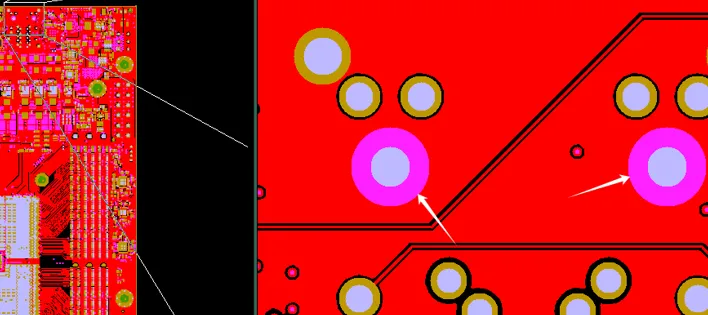
14 Layer TG170 PCB Manufacturing Review for Impedance and Resin Plugging
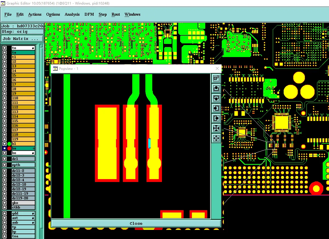
Why Your 20 Layer PCB Fails CAM: Trace Space & Impedance Fixes
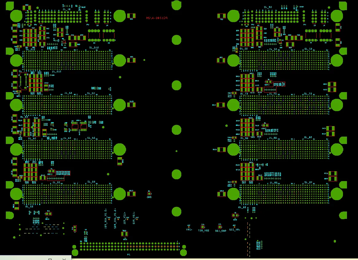
How to Resolve Backdrill, Press-Fit & Copper Balance Issues in 3mm 24-Layer FR4 PCB
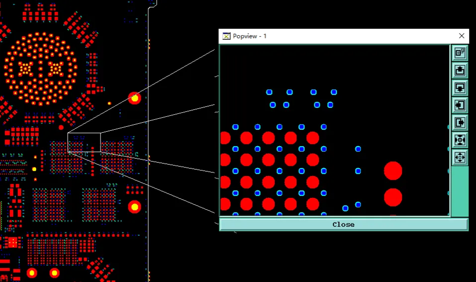
Fixing 18-Layer PCB Risks: The Power of PCB CAM Review
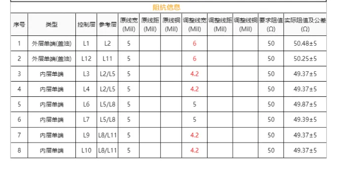
Resolving 12 layer FR4 PCB Copper Thickness and Impedance Conflicts
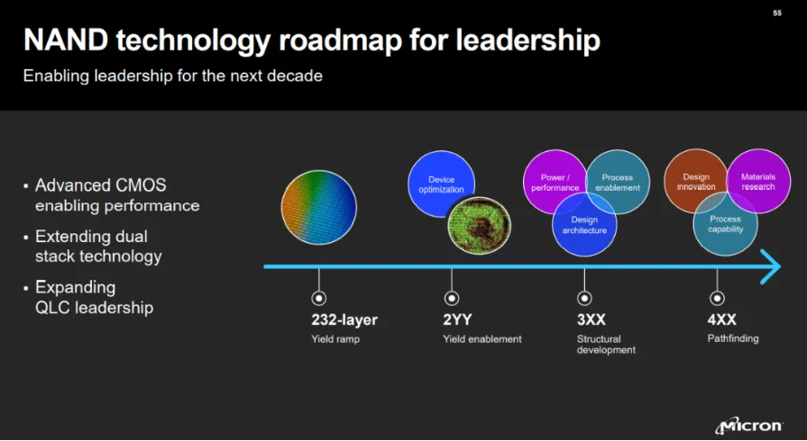
3D NAND Layer Race: 300+ Layers Arrive
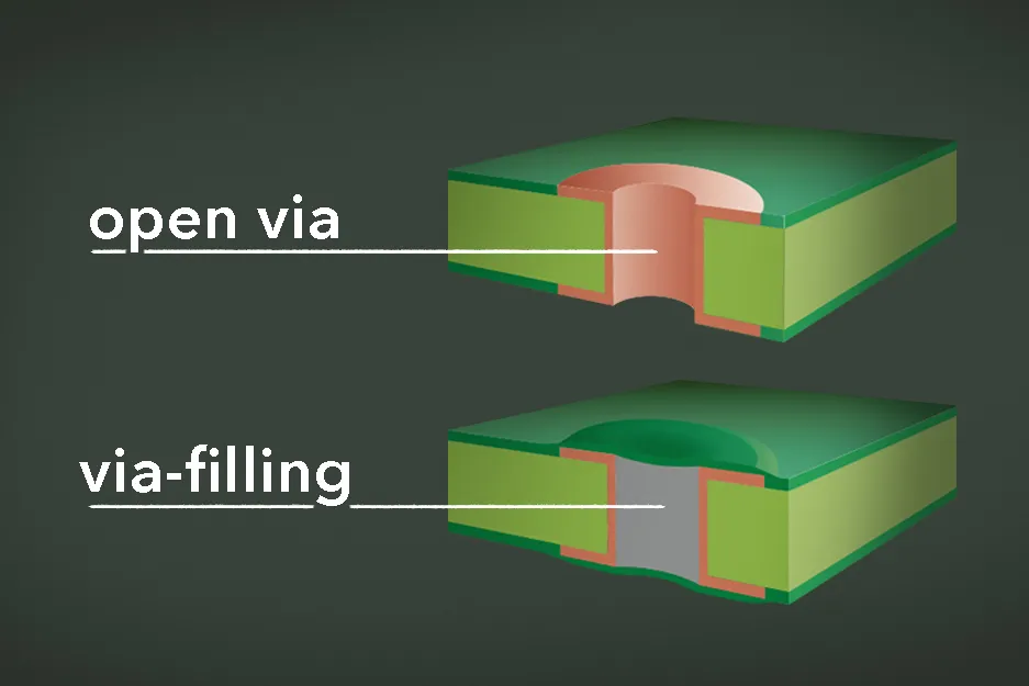
The Benefits of Using Filled Vias in High Layer Count PCBs
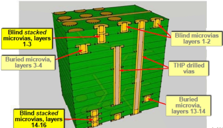
Reducing EMI in High Layer Count PCBs: Shielding and Grounding Techniques
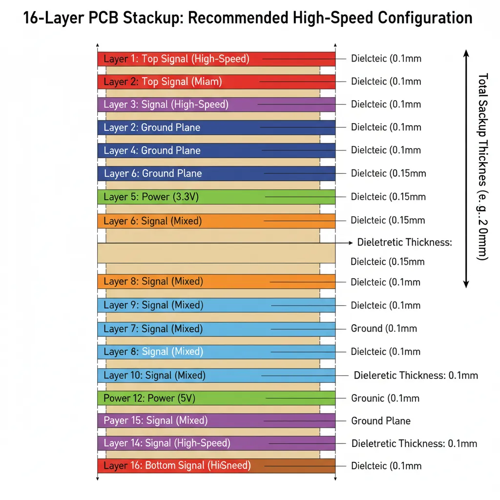
How to Design an Effective 16-Layer PCB Stackup for High-Performance Electronics
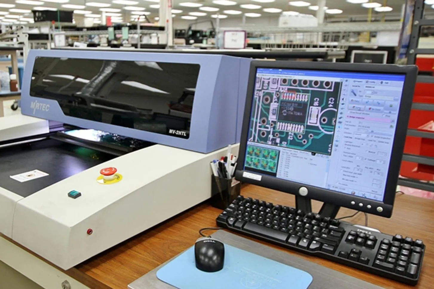
Testing and Inspection Methods for Multi-Layer PCBs: Guaranteeing Performance
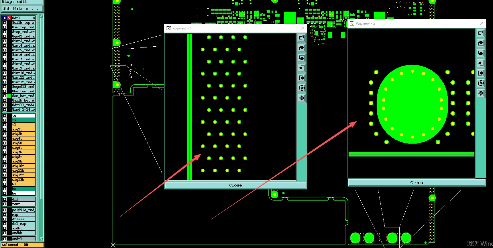
How We Resolved Resin Plug Tenting Conflict on 14-Layer PCB