










A 14-layer FR-4 board measuring 278.7 mm × 215.82 mm came in for CAM review. The order specified 2.4 mm thickness, TG170 material, 2 oz copper on all layers, red solder mask, white silkscreen, immersion gold, resin-plugged vias, and customer panelization with routing slots and zero process edge. Quantity was only 5 pieces. During data verification we found a clear conflict on the via treatment. The customer required resin plugging followed by solder-mask tenting, yet the Gerber data showed openings over the holes on the bottom layer. At the same time some guard holes were highlighted without a clear plugging instruction, and several layer names did not match the stated sequence. These mismatches left us unable to decide the correct via process. Production could not start until the resin-plug and tenting requirements were clarified.
Design Intent for Resin-Plugged and Tented Vias
The board ( #FR4-20260427-035 ) was a thick, high-layer-count design with 2 oz copper. Resin plugging is normally chosen when the surface must stay flat for fine-pitch components or for reliable immersion-gold plating. Tenting (covering the plugged vias with solder mask) further protects the via and prevents solder wicking. The customer notes explicitly called for resin plug plus cover oil. On a 14-layer, 2.4 mm board this process is critical because any open via can create voids, plating defects, or assembly problems. The design intent was therefore a fully plugged and tented via structure across the board.
Bottom-Layer Openings That Contradicted the Tenting Note
Our CAM engineer compared the fabrication notes with the actual solder-mask layers. The notes required resin plug and tenting. The bottom solder-mask Gerber, however, contained clear openings over the holes. If we followed the Gerber data the vias would remain open after plugging. If we followed the notes we would have to close those openings. Either choice changed the final surface and the reliability of the immersion-gold finish.
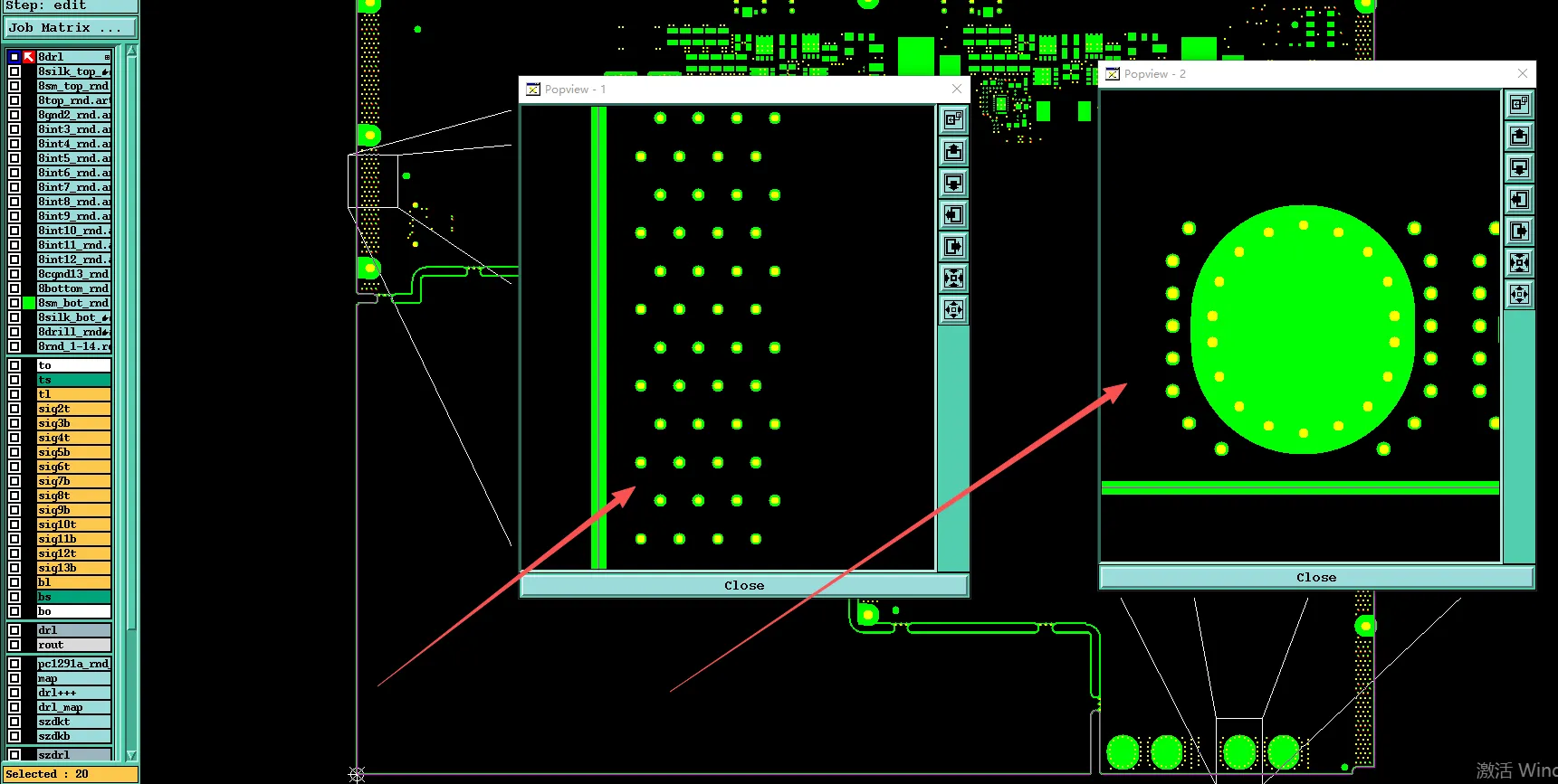
Figure 1: The notes required resin plug and tenting but the bottom solder-mask Gerber contained clear openings over the holes
Leaving the openings would allow solder or contaminants into the plugged vias during assembly. Forcing tenting without confirmation risked covering pads or features the designer intended to keep open. On a low-volume 5-piece order the cost of getting this wrong was high relative to the quantity.
| Requirement | What the Notes Said | What the Gerber Showed | Risk if Wrong |
|---|---|---|---|
| Via treatment | Resin plug + tenting | Bottom holes open | Open vias or covered pads |
| Guard holes | Not clearly defined | Highlighted in review | Inconsistent plugging |
| Layer sequence | Stated order | Names did not match | Wrong stackup interpretation |
Primary Conflict: Resin Plug Requirement Versus Mask Openings
The dominant conflict was a direct contradiction between the written via process and the Gerber solder-mask data. Resin plugging followed by tenting is a single, continuous process. When the mask layer shows openings, the factory cannot know whether the openings are intentional or an oversight. On a 14-layer board with 2 oz copper and immersion gold the surface condition after plugging is critical. Open vias can trap chemistry, create voids, or allow solder to wick during assembly. Fully tented vias keep the surface clean and flat.
We also saw guard holes highlighted in the review files without a clear plugging instruction. If some vias were to be plugged and others left open, the process window would split and increase the chance of mixed results. Layer-name inconsistencies added further uncertainty about which dielectric layers the vias passed through. Without a single, confirmed rule for every hole we could not set the plugging and mask programs.
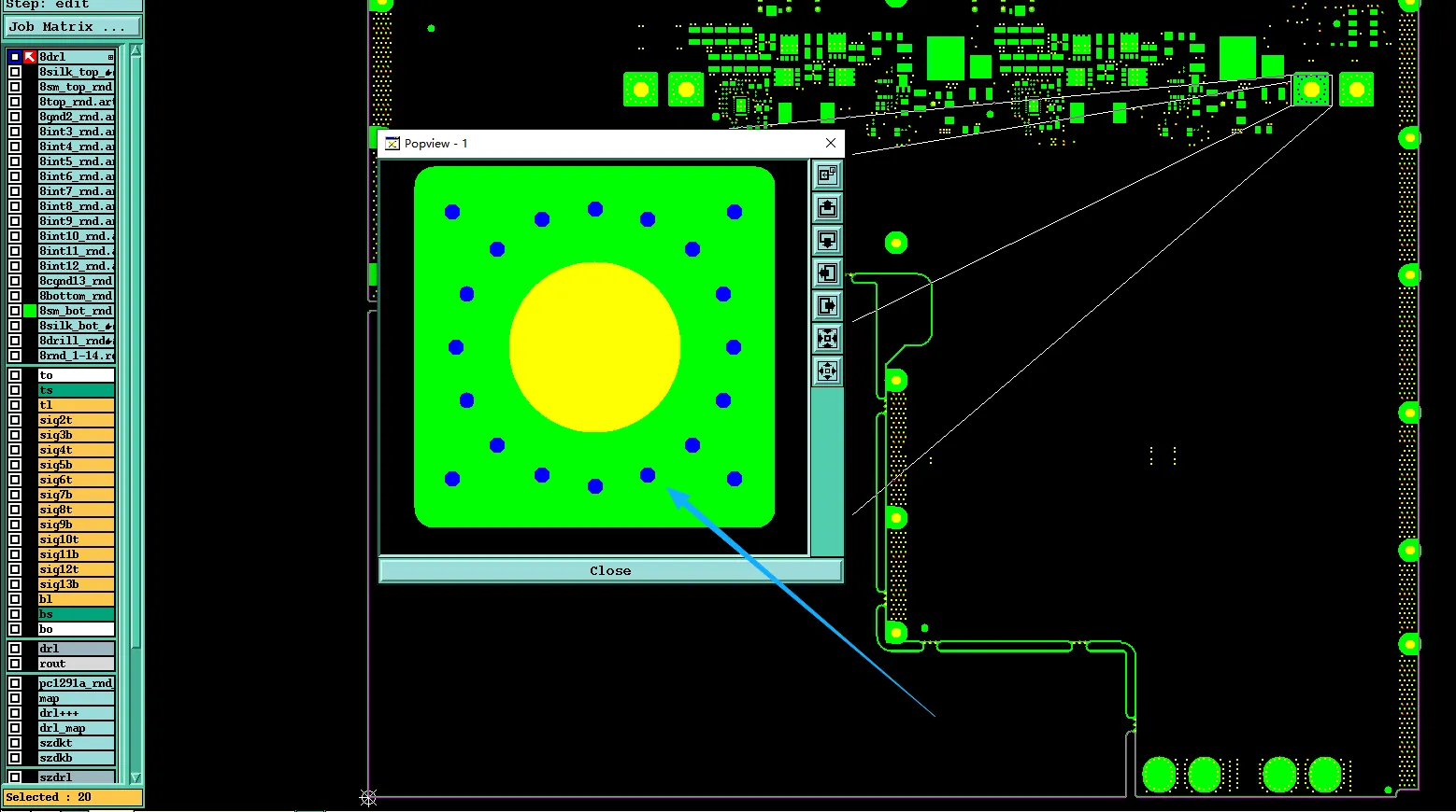
Figure 2: the blue holes indicated on the picture without a clear plugging instruction
The risk of proceeding without clarification was realistic. Boards could leave the factory with open vias that later failed at assembly, or with tented pads that the designer needed open. Either outcome would scrap a 5-piece order that already carried a 15-day lead time.
Supporting Issues on Edge Copper and Marking
While the via conflict was the main stop, three related points appeared. The customer panel had no copper on the auxiliary edge. Given our stackup and the zero process edge, we proposed pouring copper on that edge for better plating uniformity and mechanical strength. The notes also required factory number, date code, and serial numbers. We prepared a marking layout using week-of-year date code and sequential serials 01 through 05. Finally, the layer-name versus sequence mismatch needed a single authoritative order so the stackup could be locked. These items were secondary, yet each of them depended on a clean decision about the via process first.
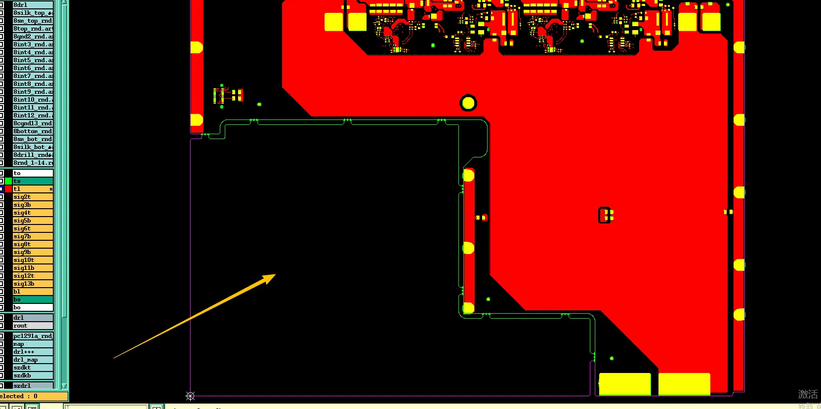
Figure 3: The customer panel had no copper on the auxiliary edge
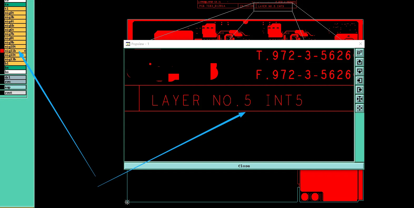
Figure 4: some layer name does not match with its descriptions
How the Via Treatment and Related Details Were Settled
We sent a clear engineering package. First, we showed the bottom-layer openings and asked whether the vias should be tented (openings closed) or left open as drawn. Second, we asked specifically about the highlighted guard holes—whether they required resin plug or should follow the same rule as the other vias. Third, we proposed copper pour on the auxiliary edge, supplied the marking layout for factory number / date code / serial, and listed the layer-name inconsistencies for correction.
The customer confirmed that all vias, including the guard holes, were to be resin-plugged and tented. The bottom-layer openings were therefore to be closed. Copper pour on the auxiliary edge was accepted. The marking layout with week-of-year date code and serials 01–05 was approved. The layer sequence was corrected to match the actual stackup. With those answers the CAM data were updated, the plugging and mask programs were set, and the 5-piece order was released.
| Observation | Conflict | Proposal | Final Decision |
|---|---|---|---|
| Bottom holes open in Gerber | Conflicts with tenting requirement | Close openings and tent all plugged vias | Approved |
| Guard holes highlighted | Plugging status unclear | Treat same as other vias | Confirmed |
| Auxiliary edge no copper | Plating and strength concern | Add copper pour | Accepted |
| Layer name vs sequence mismatch | Stackup ambiguity | Correct to actual order | Corrected |
Design Lessons for Resin-Plugged Via Boards
- When you require resin plug plus tenting, make sure the solder-mask layers show no openings over the vias. Openings contradict the tenting instruction.
- Clearly state whether every via, including guard holes or via fences, needs plugging. Mixed treatment creates process splits and higher defect risk.
- On thick, high-layer boards with heavy copper, open vias after plugging can trap chemistry or allow solder wicking. Tenting is usually the safer default.
- If the panel has zero process edge, consider copper pour on auxiliary edges for better plating uniformity and mechanical strength.
- Layer names in the Gerber set must match the stated stackup sequence. Inconsistencies force the factory to stop and ask.
- When markings such as factory number, date code, and serial are required, supply a clear location and format or accept the fabricator’s standard layout.
- Low-quantity orders still need the same via-process clarity as high-volume ones. A single wrong via treatment can scrap the entire lot.
FAQ
Q1: Why is it a problem when the notes require tenting but the Gerber shows openings over the holes?
A1: Tenting means the solder mask must cover the plugged via. Openings in the mask layer leave the via exposed, which defeats the purpose of tenting and can allow solder or contaminants inside.
Q2: What happens if some vias are plugged and others are left open?
A2: The process window splits. Different holes receive different treatments, raising the chance of inconsistent filling, voids, or surface defects.
Q3: Why do guard holes need an explicit plugging instruction?
A3: Guard holes are often placed for isolation or shielding. Without a clear note the factory cannot know whether they follow the same resin-plug rule as the signal vias.
Q4: Is copper pour on the auxiliary edge necessary when the process edge is zero?
A4: It is not always required, but it improves plating uniformity and edge strength on thick boards. The fabricator will propose it when the stackup and panel design make it beneficial.
Q5: Why must layer names match the stated sequence?
A5: CAM systems and the press program rely on a consistent layer order. Mismatched names create ambiguity about which dielectric is which and can lead to an incorrect stackup.
Q6: How can designers avoid resin-plug versus mask-opening conflicts?
A6: When the notes call for tenting, generate the solder-mask layers with no openings over the vias. State clearly that every via, including any guard holes, follows the same plugging and tenting rule.






