










A 10-layer FR-4 board measuring 324.8 mm × 76.8 mm entered CAM review with controlled impedance, resin-plugged vias, immersion gold, and gold-finger bevel. The order specified 1.6 mm thickness, TG170 material, 0.5 oz inner / 1 oz outer copper, green solder mask, white silkscreen, and a factory 1 × 2 panel with 4 mm process edges. Quantity was 30 pieces. The customer provided stackup and impedance requirements. During review we found that the differential impedance line spacing in the Gerber data did not match the stated targets. Some impedance-controlled traces were also drawn on layers that did not exist. At the same time our available materials required a small stackup adjustment. These mismatches made it impossible to guarantee the required impedance. Production could not start until the stackup and the impedance lines were brought into agreement.
Design Intent for Controlled Impedance on 10 Layers
The board ( #FR4-20260720-046 ) was a 10-layer design built for controlled impedance and gold-finger connections. Resin-plugged vias and immersion gold indicated a need for flat surfaces and reliable high-speed signal paths. The customer supplied both a target stackup and specific differential impedance values. The design goal was consistent impedance performance across the differential pairs. In a clean data package the stackup, line widths, and spacings work together to hit those targets. Here they did not line up.
Differential Line Spacing That Missed the Target
Our CAM engineer compared the impedance notes with the actual Gerber data. The required differential impedance called for a defined line width and spacing. The traces in the files used a different spacing. In several locations the impedance-controlled lines sat on layers that did not exist in the 10-layer stack. The customer's stackup drawing also assumed materials we did not carry. We had to adjust the core and prepreg combination to match available TG170 stock. That change altered the dielectric thicknesses and therefore the impedance calculation.
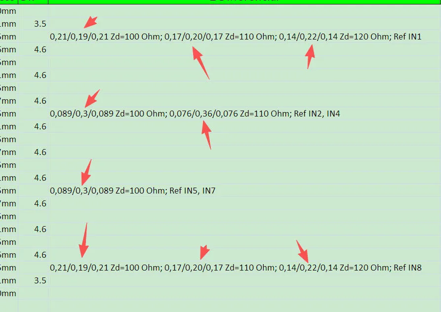
Figure 1: some impedance lines are missing on their corresponding layers
If we had built the board with the original spacing and the original stackup, the finished impedance would have fallen outside the target. High-speed signals would have seen reflections, timing skew, or excess loss. On a board that already carried gold fingers and resin-plugged vias, those signal-integrity problems would have been costly to find at assembly.
| Item | Customer Requirement | What the Files Showed | Risk |
|---|---|---|---|
| Differential spacing | Specified value | Different value in Gerber | Impedance out of tolerance |
| Impedance layer assignment | Defined layers | Some lines on non-existent layers | Uncontrollable impedance |
| Stackup materials | Customer drawing | Required material adjustment | Dielectric thickness shift |
Impedance Rules Clashing with Trace Geometry and Stackup
The core conflict sat between three elements: the impedance targets, the physical traces in the Gerber files, and the stackup we could actually build. Impedance is set by line width, spacing, dielectric thickness, and dielectric constant. In this design the spacing in the files did not match the calculation, and some traces were placed on layers that did not exist. At the same time the available materials forced a small change in dielectric thickness. Together these issues made it impossible to guarantee the required differential impedance.
We could not ignore the spacing error. Building the board as drawn would have produced impedance values outside the customer's window. We also could not change the traces without approval, because the geometry might have been intentional for routing density. The only safe route was to show the exact differences, propose a revised stackup that matched our materials, and ask for confirmation on both the stackup and the line spacing.
The impedance notes also lacked a tolerance. Without a tolerance we had no way to judge how much deviation was acceptable. That missing detail added another reason to stop and confirm before tooling began.
Additional Issues with Layers and Production Draft
While the impedance conflict was the main blocker, two related points appeared. The customer had supplied a production draft and asked us to confirm it. We treated that draft as the reference for outline and gold-finger details. The order also required resin-plugged vias and gold-finger bevel. Both features interact with surface flatness and edge quality. These items were secondary, but they underlined the need for a clean, confirmed data package before the 20-day lead time started to run.
How Stackup and Spacing Were Finally Aligned
We prepared a short engineering reply. First, we attached our revised stackup design that used available TG170 materials and showed the new dielectric thicknesses. Second, we listed every differential pair whose spacing did not match the impedance calculation and noted the layers that did not exist. Third, we asked the customer to confirm whether the spacing should be corrected to hit the target impedance or whether the original geometry should be kept and the impedance target relaxed.
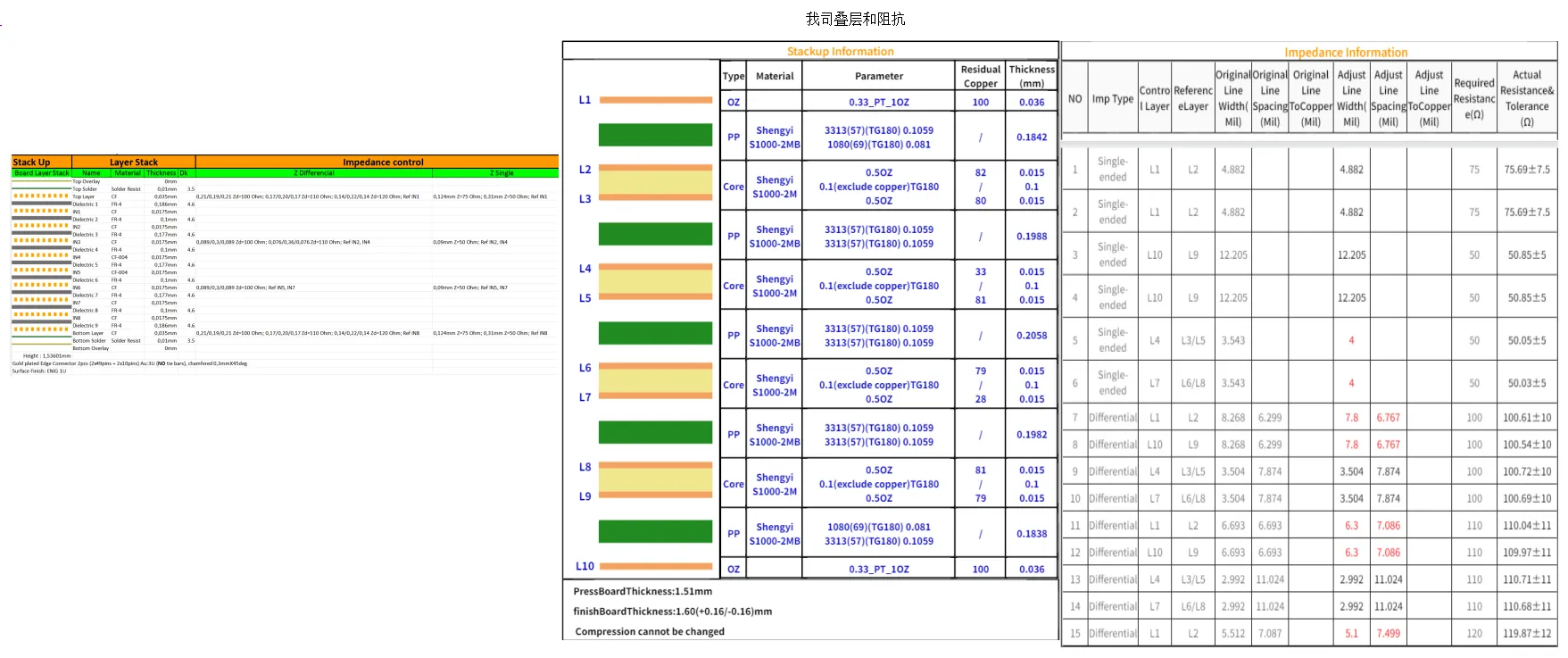
Figure 2: adjustments to the impedance and layer stack-up
The customer approved the adjusted stackup and authorized the line-spacing corrections needed to meet the differential impedance targets. References to non-existent layers were removed. With those answers in hand we updated the CAM data, locked the stackup, and released the 15-panel order for production.
| Observation | Conflict | Proposal | Final Decision |
|---|---|---|---|
| Differential spacing mismatch | Impedance out of target | Correct spacing to match calculation | Approved |
| Traces on non-existent layers | Uncontrollable impedance | Remove invalid layer references | Confirmed |
| Material-driven stackup change | Dielectric thickness shift | Supply revised stackup for approval | Accepted |
Key Lessons for Impedance-Controlled PCB Designs
- When you specify differential impedance, make sure the line width and spacing in the Gerber files match the calculation for the intended stackup.
- Never assign impedance-controlled traces to layers that do not exist in the stackup. Those lines cannot be controlled.
- If the fabricator may need to adjust materials, supply a tolerance on both impedance and finished thickness so small changes stay acceptable.
- Include the stackup drawing and the impedance table in the same data package so CAM can check them against each other.
- Gold-finger and resin-plugged via designs already constrain surface flatness. Adding uncontrolled impedance only raises the chance of late discoveries.
- Always state an impedance tolerance. A target without a window forces the factory to stop and ask.
- When the stackup must change because of material availability, the fabricator should show the new dielectric thicknesses and the recalculated impedance before proceeding.
FAQ
Q1: Why does a spacing mismatch between the impedance note and the Gerber data matter?
A1: Impedance depends on width, spacing, and dielectric thickness. If the spacing in the files is wrong, the finished value will miss the target even if the stackup is correct.
Q2: What happens when impedance lines are drawn on layers that do not exist?
A2: Those traces cannot be controlled. The factory has no dielectric reference for them, so the impedance is undefined.
Q3: Why must the fabricator confirm a material-driven stackup change?
A3: Different cores and prepregs press to different thicknesses and have different dielectric constants. Even a small change alters the impedance calculation. The customer must approve the new numbers.
Q4: Can the factory simply adjust the line spacing without asking?
A4: No. Changing geometry may affect routing density or crosstalk. Any correction needs customer approval.
Q5: Why is an impedance tolerance important?
A5: Real boards always have some variation. Without a tolerance the factory cannot decide whether a small deviation is acceptable or requires a redesign.
Q6: How can designers avoid impedance confirmation delays?
A6: Make sure the Gerber spacing matches the impedance calculation for the intended stackup. Assign traces only to real layers. Include both the stackup and the impedance table in the same package, and always state a tolerance.






