 00:47
00:47
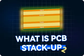
PCB Stackup Design
PCB stackup design is a fundamental aspect of printed circuit board engineering that determines the arrangement of conductive and insulating layers within a PCB. This configuration plays a critical role in ensuring signal integrity, managing electromagnetic interference, and optimizing thermal performance in electronic devices. For engineers and designers searching for insights on PCB stackup design, this tag aggregates resources that delve into the principles and methodologies for creating effective multilayer boards, from simple two-layer setups to complex high-speed applications. Understanding PCB stackup design begins with selecting appropriate layer counts, materials, and via structures to meet specific project requirements. Key considerations include controlled impedance for high-frequency signals, power distribution planes to minimize noise, and ground layers for shielding. Practical applications span industries such as telecommunications, automotive electronics, and consumer gadgets, where poor stackup can lead to issues like crosstalk or signal degradation. Best practices emphasize simulation tools for pre-layout analysis, adherence to manufacturing constraints, and iterative testing to refine designs, ultimately reducing prototyping costs and time to market. Articles under this tag offer detailed guides on topics like symmetric versus asymmetric stackups, the impact of dielectric constants on performance, and strategies for high-density interconnects. Whether you are troubleshooting a current project or planning a new one, these resources provide actionable steps to enhance your PCB designs. Dive into the collection to find case studies, tutorials, and expert tips that align with real-world challenges in electronics development.
Video Guide

Technical Articles
Mastering Rogers PCB: A Comprehensive Resource for High-Speed Design, Applications, and Fabrication
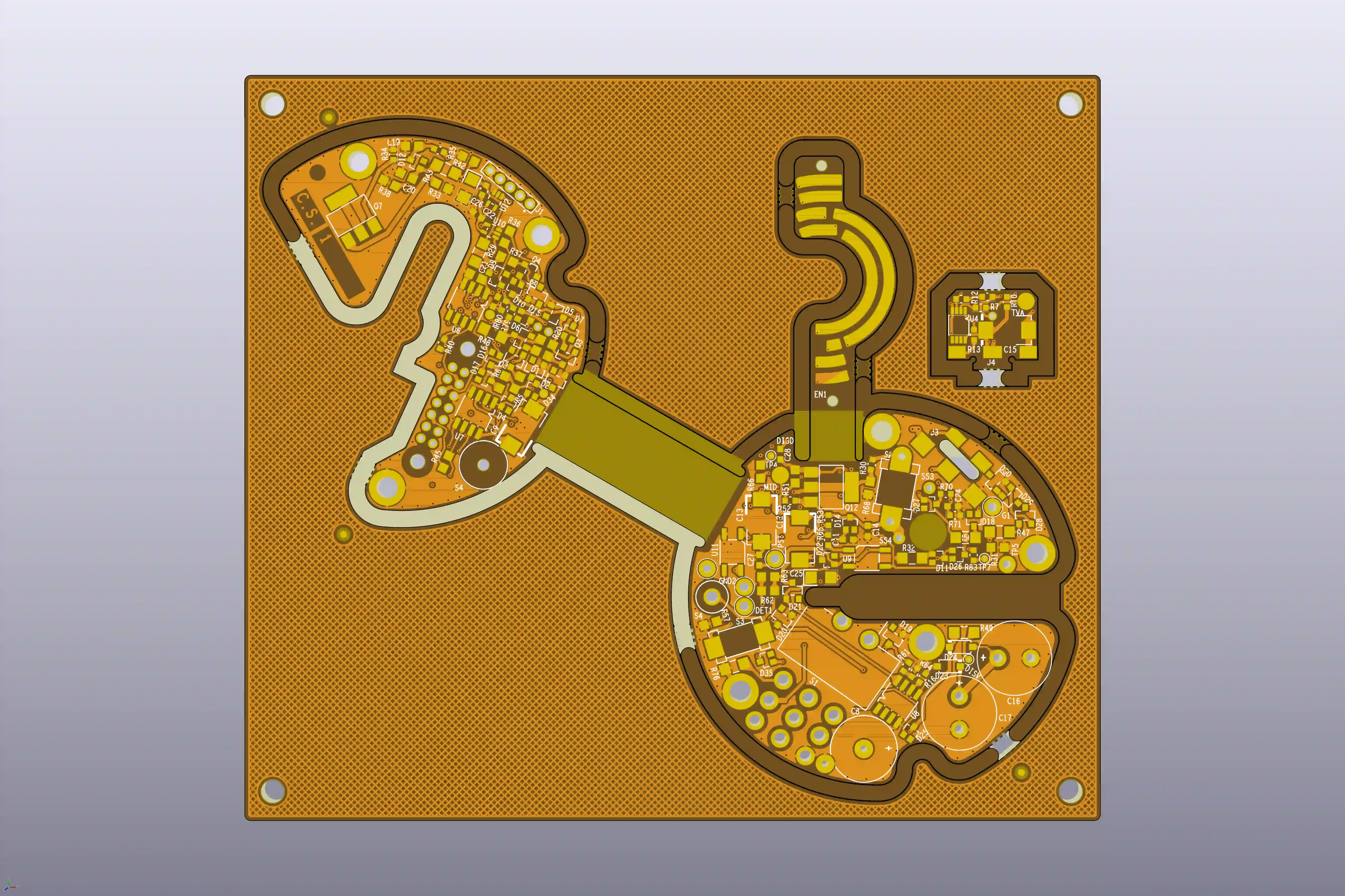
Rigid-Flex PCBs: The Ultimate Solution for Complex Wearable Health Monitors
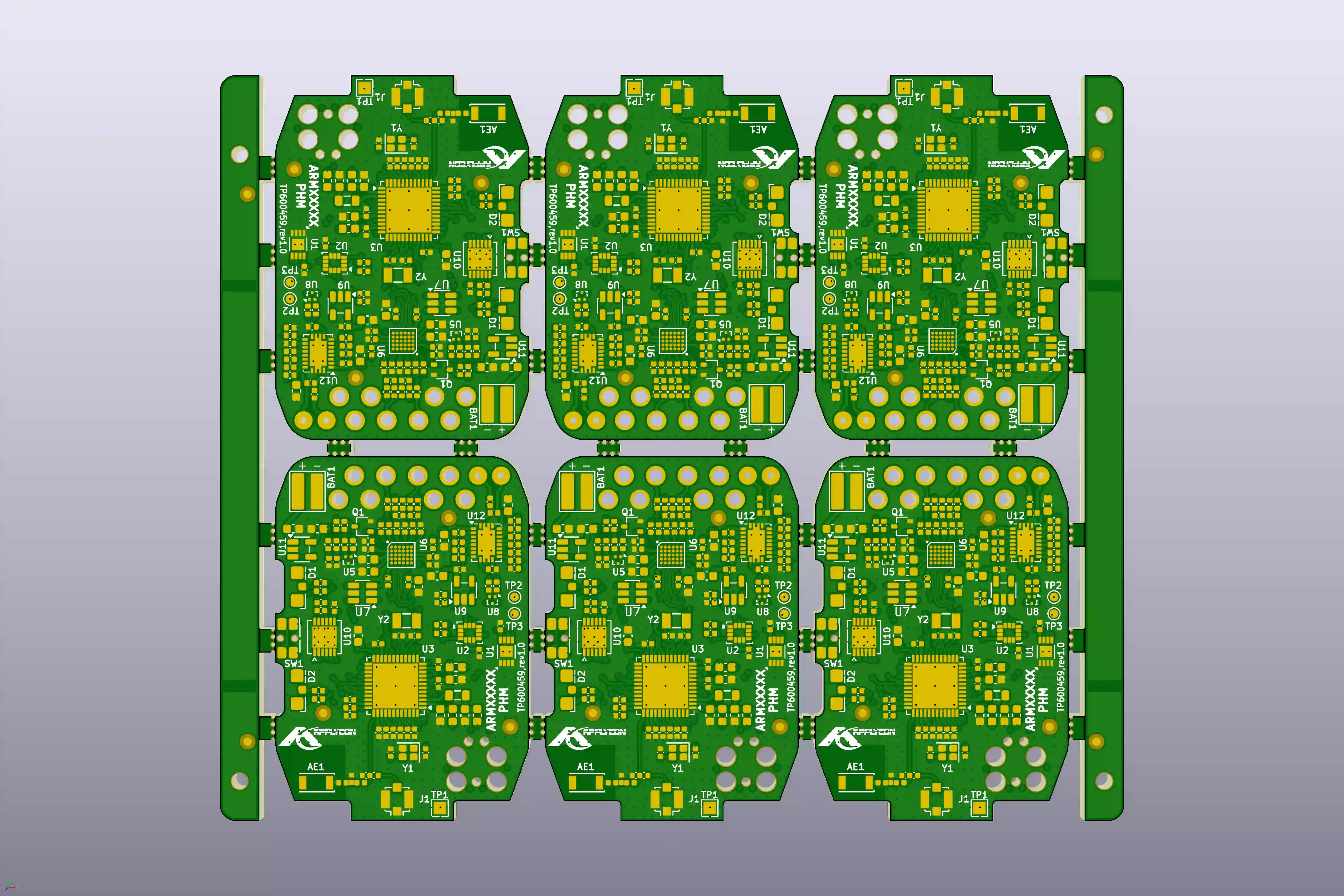
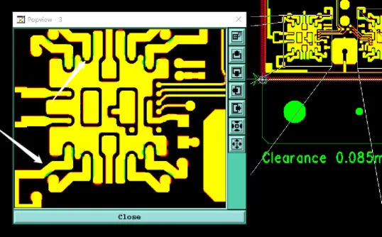
18-Layer 2.0mm FR-4 PCB Case Study: Critical Impedance and Stackup Issues Discovered During CAM Engineering Review
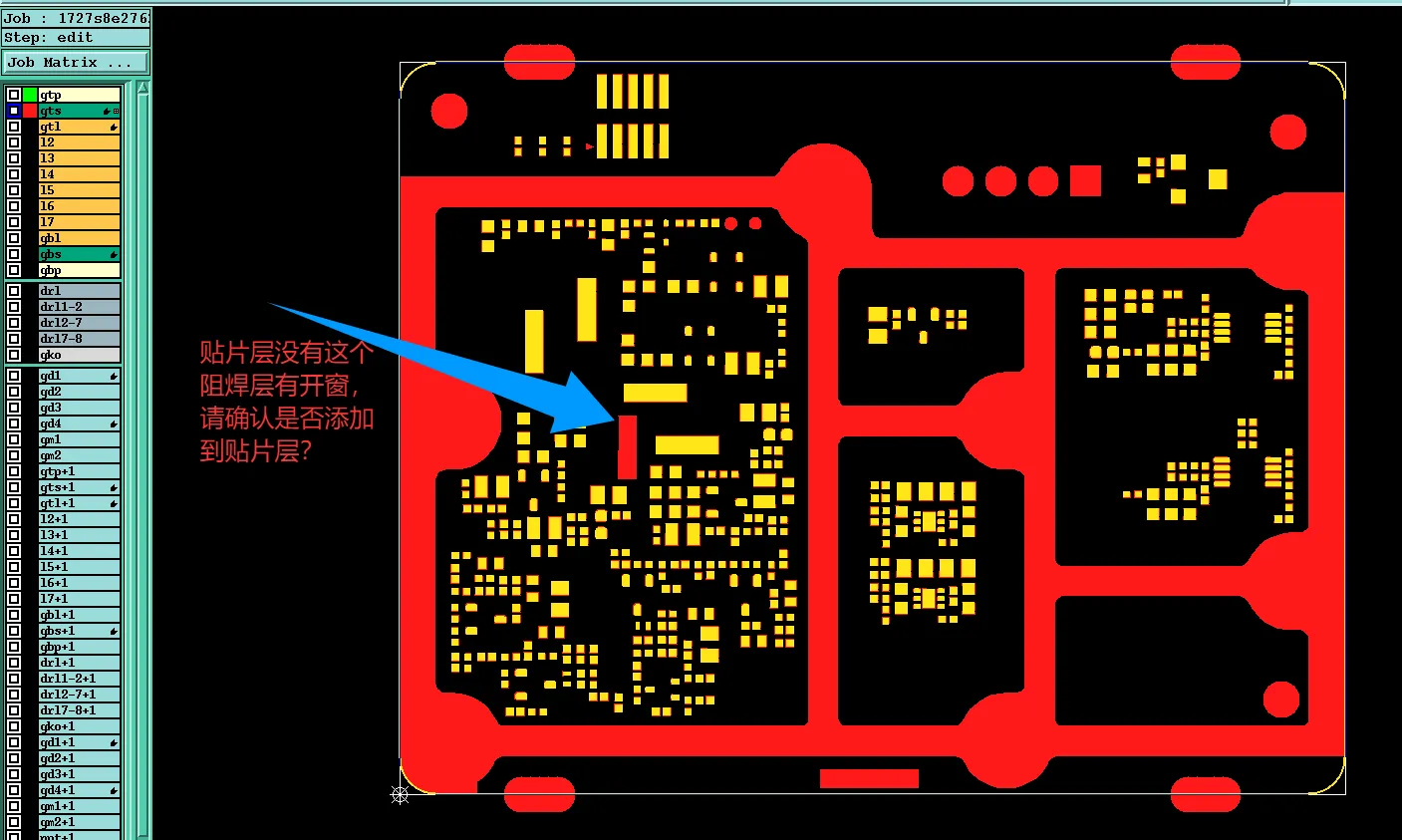
How to Avoid Common Solder Mask & Stackup Issues in 6-Layer HDI PCBs
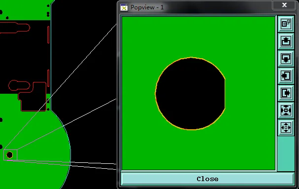
How to Avoid Edge Clearance and Via Plugging Issues in 4-Layer Rigid-Flex PCB
14 Layer TG170 PCB Manufacturing Review for Impedance and Resin Plugging
Why Your 20 Layer PCB Fails CAM: Trace Space & Impedance Fixes
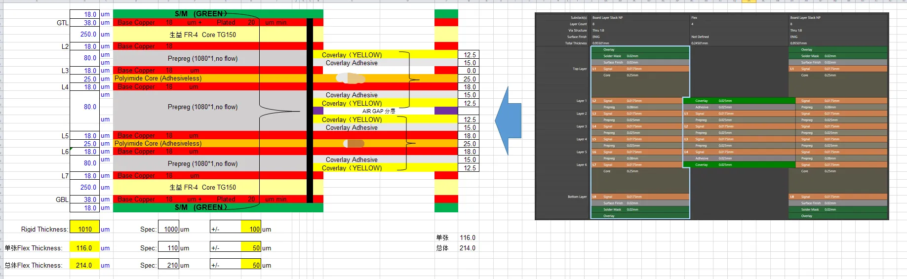
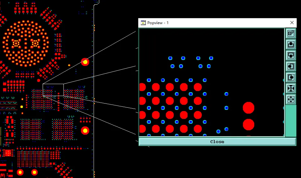
Rigid-Flex 8-Layer PCB CAM Review: Stackup Confirmation and Via-in-Pad Filling Challenges
8-Layer FR-4 TG170 Blind Via PCB: Real CAM Engineering Review Case on Stackup Optimization and Process Edge Confirmation
How to Prevent Buried Via Plating and Stackup Mismatch Issues in 8-Layer TG170 PCB
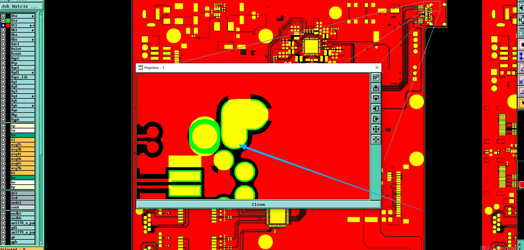
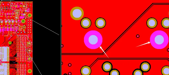
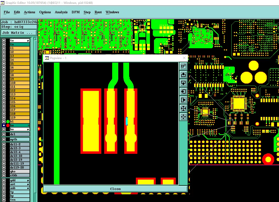
How to Fix Tight Pad Spacing and Impedance EQs in 8-Layer PCB CAM Review
How We Resolved Stackup Warpage, Blind Via Spacing & No-Mask Conflicts in Hybrid Rogers RF PCB
How to Avoid Countersink & Copper Issues in 3mm Thick FR4 PCB Manufacturing
Fixing 18-Layer PCB Risks: The Power of PCB CAM Review

Optimizing EMI Shielding in Consumer Electronics for Regulatory Compliance

Differential Signaling and Jitter: PCB Layout Techniques for Optimal Performance

Understanding the Role of Antennas in Smart Watch PCB Design

EMI Shielding Solutions for High Speed Data Transmission

Cost Effective Strategies for High Speed PCB Manufacturing: Balancing Performance and Budget
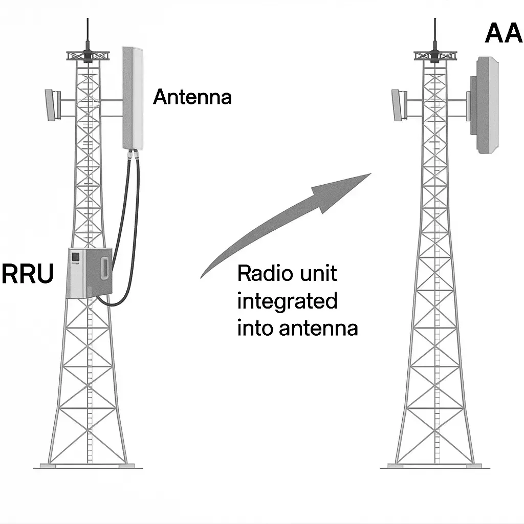
How Are 5G Base Stations Installed?
Get in Touch
Send Message
- Products & Service
- Company
- About AIVON
- Contact
- News
- Blog
- Certification
-


- Payment
-


2026 AIVON.COM All Rights Reserved