 00:47
00:47
PCB Stackup Design
PCB stackup design is a fundamental aspect of printed circuit board engineering that determines the arrangement of conductive and insulating layers within a PCB. This configuration plays a critical role in ensuring signal integrity, managing electromagnetic interference, and optimizing thermal performance in electronic devices. For engineers and designers searching for insights on PCB stackup design, this tag aggregates resources that delve into the principles and methodologies for creating effective multilayer boards, from simple two-layer setups to complex high-speed applications. Understanding PCB stackup design begins with selecting appropriate layer counts, materials, and via structures to meet specific project requirements. Key considerations include controlled impedance for high-frequency signals, power distribution planes to minimize noise, and ground layers for shielding. Practical applications span industries such as telecommunications, automotive electronics, and consumer gadgets, where poor stackup can lead to issues like crosstalk or signal degradation. Best practices emphasize simulation tools for pre-layout analysis, adherence to manufacturing constraints, and iterative testing to refine designs, ultimately reducing prototyping costs and time to market. Articles under this tag offer detailed guides on topics like symmetric versus asymmetric stackups, the impact of dielectric constants on performance, and strategies for high-density interconnects. Whether you are troubleshooting a current project or planning a new one, these resources provide actionable steps to enhance your PCB designs. Dive into the collection to find case studies, tutorials, and expert tips that align with real-world challenges in electronics development.
Video Guide

Technical Articles
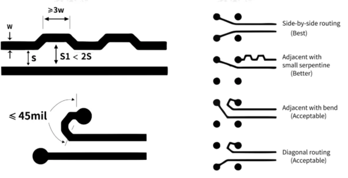
PCB Layout and Routing Requirements for a DP 1.4 Interface
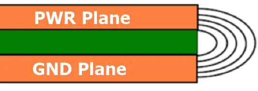
Why the Power Plane Should Be Smaller Than the Ground Plane
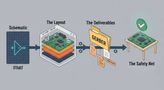
Basic PCB Concepts Needed to Start a Design
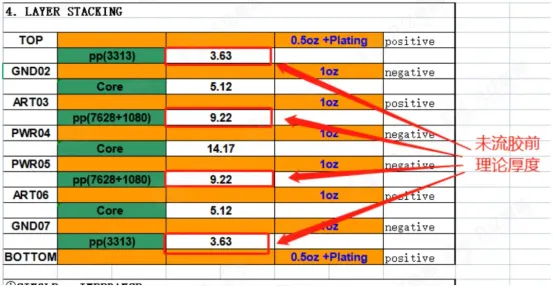
How PCB Copper Thickness Affects Current, Heat, and Strength
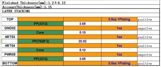
PCB Impedance Calculation for Signal Integrity
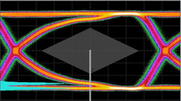
High-Speed PCB Design: From Signal Integrity to Transmission-Line Basics
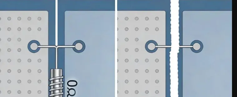
After Designing 10 PCBs: If the Layers Are Wrong, the Board Is Wasted

PCB Mass Production image
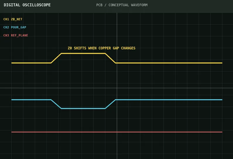
Why Impedance Changes After Adjacent Copper Pour Even When Trace Width Does Not
PCB Design Keep Going Wrong? 13 Key Fundamentals That Build a Solid Baseline
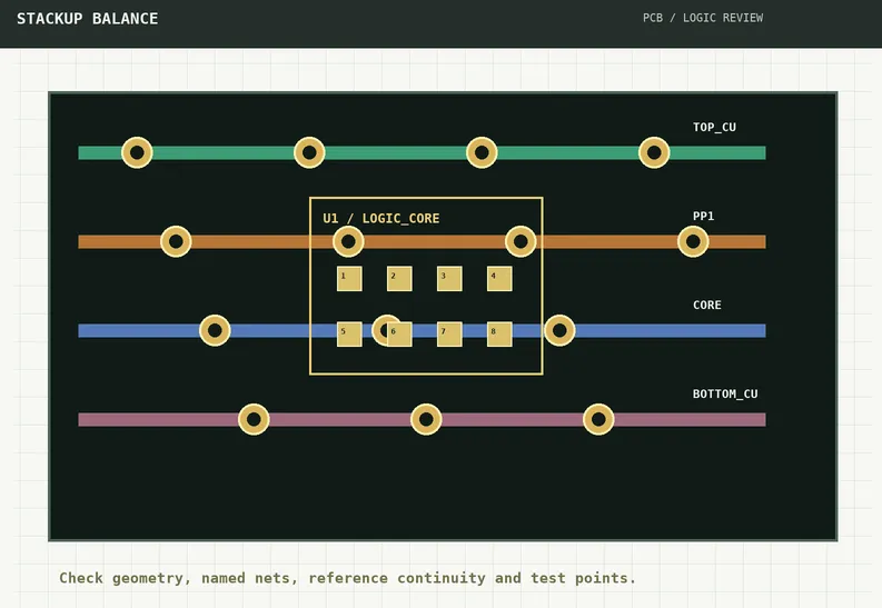
Why a PCB Still Warps When Copper Thickness Is the Same but the Stackup Is Asymmetric
Why Backdrill Stubs Can Still Be Too Long After the Layer Pair Is Correct
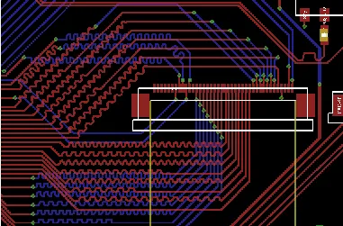
FR4 PCB Differential Pair Routing: Spacing and Length Matching
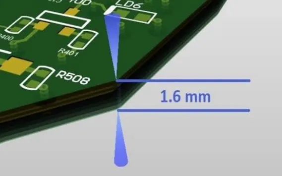
Why Does a 1.6 mm PCB Measure Only 1.4 mm? The Engineering Reality Behind PCB Thickness Calculations

Multilayer PCB Construction Explained: Layers, Cores, Prepreg and Copper Foil
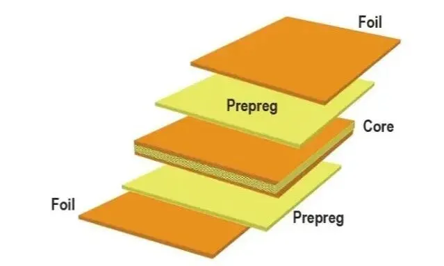
What Do 7628, 1080, and 2116 Mean in a PCB? Understanding These Numbers Means Understanding the Stack-Up
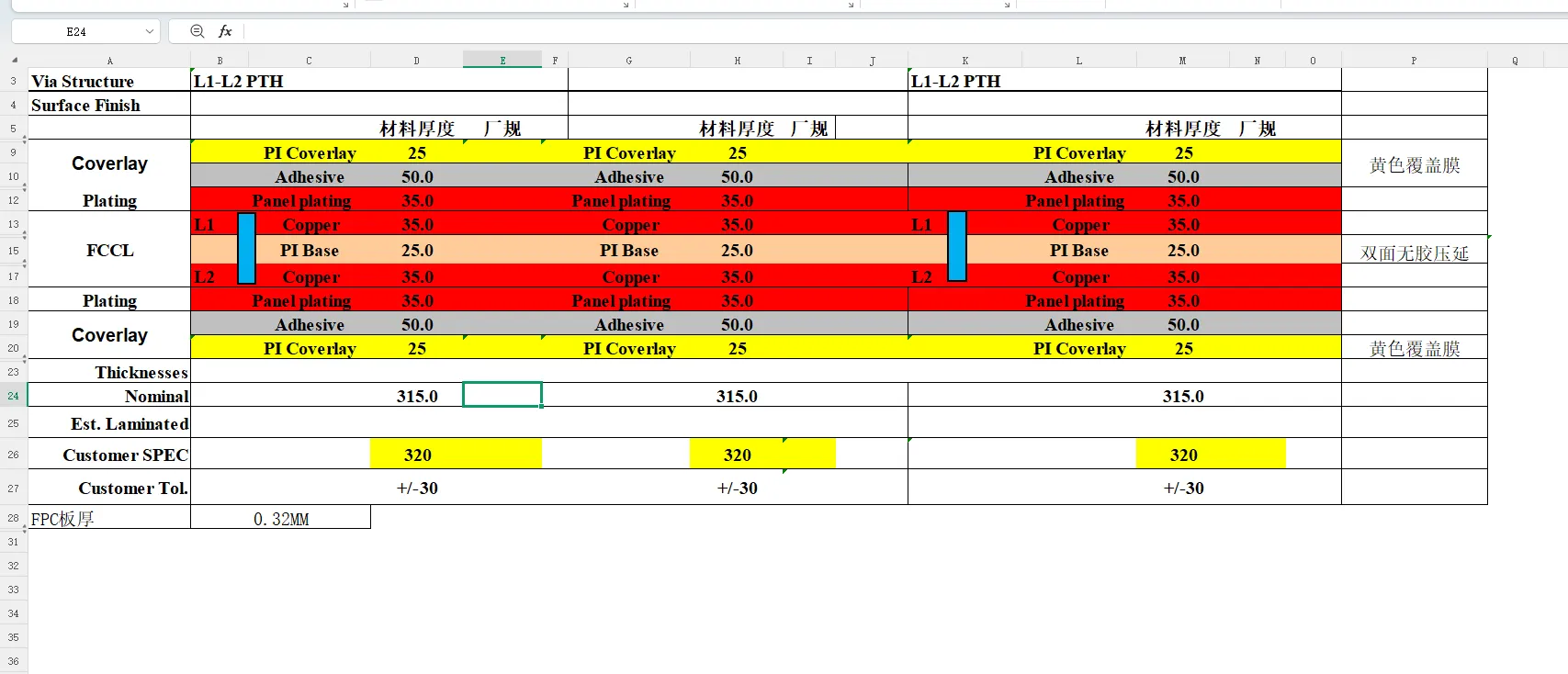
Adhesive Specification and Silkscreen Overlap in 2-Layer Flexible Circuit CAM Review
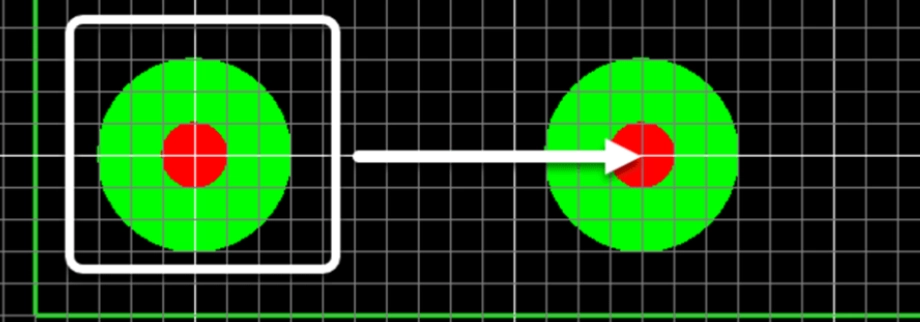
CAM Confirmation of Fiducial Marks on a 205 × 20 mm 6-Layer Rigid-Flex Panel

How AI Can Assist Multilayer PCB Routing and Design