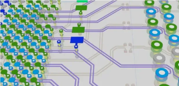
FR-4 and Tg
FR-4 is a glass-epoxy copper-clad laminate, one of the standard PCB base materials. It is grouped into standard FR-4 and high-Tg FR-4. Tg is the glass-transition temperature, the point at which the material softens. A circuit board must be flame resistant: at a given temperature it must not burn, only soften. That temperature is the glass-transition temperature (Tg) and is tied to the dimensional stability of the PCB.
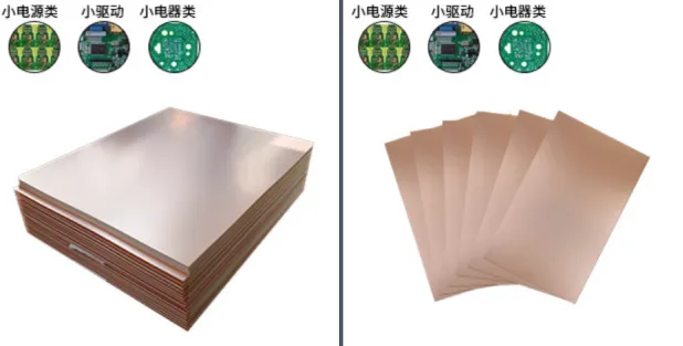
Standard-Tg material is typically 130 °C and above, high Tg is generally greater than 170 °C, and mid Tg is about 150 °C and above. A PCB with Tg ≥ 170 °C is called a high-Tg board. Raising the substrate Tg improves heat resistance, moisture resistance, chemical resistance, and stability. The higher the Tg, the better the temperature performance of the laminate. High-Tg material is used especially often in lead-free processes.
Impedance Matching
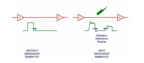
Impedance matching is used mainly on transmission lines so that high-frequency microwave energy reaches the load and almost none of the signal reflects back to the source, which improves energy transfer. When the source internal resistance equals the characteristic impedance of the attached line in both magnitude and phase, or when the line characteristic impedance equals the attached load impedance in both magnitude and phase, the input or output of the line is in an impedance-matched state. That condition is called impedance matching. Common controlled-impedance values on a PCB are 100 Ω differential, 90 Ω differential, and 50 Ω single-ended.
PCB Surface Finishes
PCB surface finishes fall into several types. A short comparison helps when choosing a finish for a given design.
-
HASL (hot-air solder leveling)
HASL is the most common surface finish in board fabrication. Solderability is good, and it can be used on most electronic products. Compared with other finishes it is low in cost and solders well. The drawback is that the surface is not as flat as immersion gold. Uneven solder is more likely when large areas are opened in the mask.
-
Immersion tin
Immersion tin differs from HASL in that the surface is flatter. The drawback is that it oxidizes and darkens easily.
-
Immersion gold (ENIG)
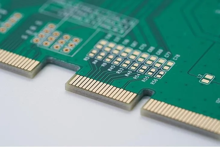
Any "immersion" finish is flatter than a "spray" or HASL process. Immersion gold is lead-free. It is commonly used on gold fingers and keypad boards, because gold has low resistance and is required on contact surfaces, such as phone keypad boards. Immersion gold is soft gold. Parts that are plugged and unplugged often should use electroplated gold. Immersion gold is primarily electroless nickel immersion gold.
-
Electroplated gold
Electroplated gold was already noted under immersion gold. A serious drawback is poor solderability, but it is harder than immersion gold. This finish is generally not used in MID and VR designs.
If flatness matters, such as on impedance-controlled boards that are sensitive to frequency (for example microstrip), prefer immersion gold. MID boards that include BGAs also typically use immersion gold.
-
OSP
OSP forms a solderable film by a chemical reaction with the copper to be soldered. Its only advantages are short process time and low cost. Solderability is poor and the finish oxidizes easily, so it is used less often in board fabrication.
Copper-Clad Laminate, Core, and Prepreg
A sheet made by impregnating reinforcement with resin, cladding one or both sides with copper foil, and pressing under heat is called a copper-clad laminate (CCL). It is the basic material for a PCB and is often called the base material. When it is used to build a multilayer board, it is also called the core.
A sheet bonding material made from resin and a carrier is called prepreg (PP).
Core and prepreg are the usual materials used to laminate a multilayer board.
Differential Signals
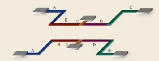
A differential signal is two equal-amplitude, opposite-polarity signals sent from the driver. The receiver compares the voltage difference to decide logic 0 or 1. The pair of traces that carries that signal is a differential pair. Differential signaling, sometimes called a differential-mode signal, sends one data path on two identical, opposite-polarity lines and decides the bit from the level difference. To keep the two signals the same, the traces must stay parallel in routing, with constant width and spacing.
Signal Integrity
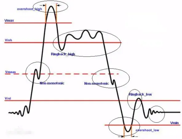
Signal integrity is the quality of a signal on a transmission line. Good signal integrity means the voltage reaches the required level at the required time. Poor signal integrity is not caused by one factor alone; it comes from several board-level effects acting together. The main signal-integrity problems include reflection, ringing, ground bounce, and crosstalk.
Reflection
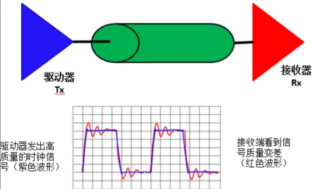
Reflection is the echo on a transmission line. Part of the signal power (voltage and current) travels down the line and reaches the load, and part is reflected. If the source and the load have the same impedance, reflection does not occur. A mismatch between source and load impedance causes reflection on the line, and the load sends part of the voltage back toward the source. If the load impedance is less than the source impedance, the reflected voltage is negative. If the load impedance is greater than the source impedance, the reflected voltage is positive. Changes in trace geometry, incorrect termination, travel through a connector, and discontinuities in the power plane can all produce this kind of reflection.
Reflection causes overshoot, undershoot, ringing, and slowed edges, which appear as a stepped voltage waveform.
Crosstalk
Crosstalk is coupling between two signal traces. Mutual inductance and mutual capacitance between the traces produce noise on the victim line. Capacitive coupling produces a coupled current; inductive coupling produces a coupled voltage. PCB stack-up parameters, trace spacing, the electrical characteristics of the driver and receiver, and the termination method all affect crosstalk.
Internal Planes
An internal plane is a negative-image layer in the PCB. Its main use is as a power or ground layer, with plane splits added when needed.
Blind Vias and Buried Vias
- Blind via: a via that runs from an inner layer to one outer surface of the PCB. These are often described by order, such as first-order or second-order. A first-order blind via is a via from layer 2 to the top layer, or from the second-to-last layer to the bottom layer.
- Buried via: a via from one inner layer to another inner layer. It does not reach either outer surface of the PCB.
Pads, Fingers, and Test Points
These typically include standalone PTH holes, SMT pads, gold fingers, bonding fingers, IC fingers, BGA solder joints, and customer test points used after through-hole assembly.
Fiducials (Mark Points)
A mark point is a position-recognition feature used by an automatic pick-and-place machine. It is also called an optical fiducial. The choice of fiducial directly affects placement efficiency. Which mark to use generally depends on the placement machine. A mark point is typically designed as a Φ 1 mm (40 mil) circle. To keep contrast between the material color and the surroundings, leave a solder-mask-free area 0.5 mm (19.7 mil) larger than the optical fiducial, with no text in that area, as shown in the figure. On the same board, the optical fiducials must have the same inner-layer background: all three marks should either have copper under them or all should have none. An isolated optical fiducial with no routing within 10 mm should have a protective ring with a 2 mm inner diameter and 1 mm ring width, plus an octagonal isolation copper ring whose upper and lower sides are 2.8 mm across.
Plated and Non-Plated Holes
A hole with metal deposited on the barrel is a plated hole. It is used mainly for electrical connection between conductive patterns on different layers. A hole without plating is a non-plated hole and is generally used as a tooling hole or a mounting hole.