Via stitching is a practical technique used to tie copper pours together through the PCB stackup, provide low-impedance return paths, reduce loop area, improve shielding effectiveness, and enhance heat spreading. In KiCad, the kicad-action-scripts plugin offers a fast, repeatable way to populate stitching vias within defined copper zones, saving manual effort and ensuring a consistent pattern across the board.
This article explains what the plugin provides, how to install and run it, the meaning of its configuration options, and practical considerations for using via stitching effectively in real designs.
Plugin Overview
The kicad-action-scripts package includes two tools:
- Via Stitching: populates stitching vias across selected copper zones.
- Add Circular Copper: creates circular copper features.
This guide focuses on the Via Stitching tool. It can quickly and conveniently place stitching vias in bulk within selected copper zones according to the rules you specify.
Repository name: jsreynaud/kicad-action-scripts
Installation
You can install the plugin directly from KiCad's Plugin and Content Manager. Search for kicad-action-scripts, install it, and enable it in PCB Editor. Alternatively, you can install it from a local file package using KiCad's "Install from file" function.
Running the Via Stitching Tool
After installation, launch the Via Stitching Generator from the toolbar icon or via Tools → External Plugins → Via Stitching Generator.
Important: stitching vias must connect to a plane or copper pour. Before running the plugin, ensure the target area is covered by a copper zone and that the zone is poured (refreshed).
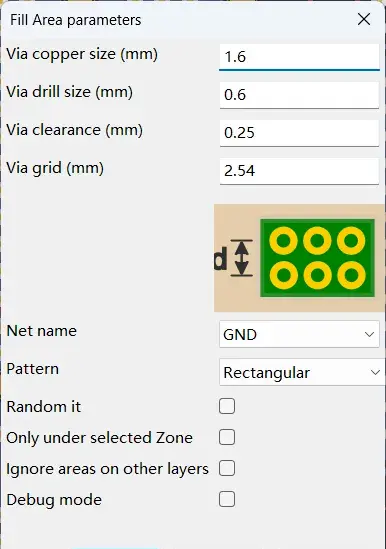
The configuration dialog is shown below:
Configuration Options
- Via copper size (mm): the via's overall diameter (pad outer diameter).
- Via drill size (mm): the plated drill hole diameter.
- Via clearance (mm): the clearance from the stitching via to other copper. Note: this function is not fully complete and may have issues; verify clearances with DRC.
- Via grid (mm): spacing between stitching vias (labeled d in the figure). This sets the array pitch.
- Net name: the target net for the stitching vias. All nets associated with existing copper zones can be selected (commonly GND).
- Pattern: the stitching pattern. Random it: randomly selects a stitching pattern.
- Only under selected Zone: when checked, vias are added only to the currently selected copper zone.
- Ignore areas on other layer: ignores conflicting areas on other layers during placement.
- Debug mode: when running from the command line, enables printing of debug information.
Example and Results
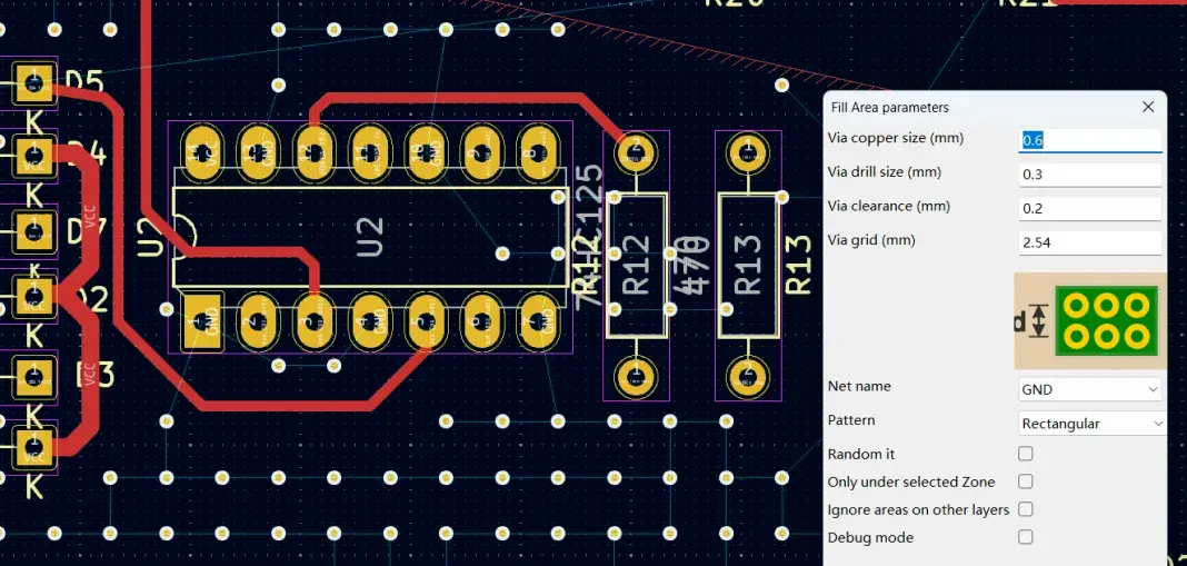
The example below shows stitching vias added to a GND copper zone in a sample project. The plugin automatically avoids footprints, tracks, and other electrical objects when placing vias.
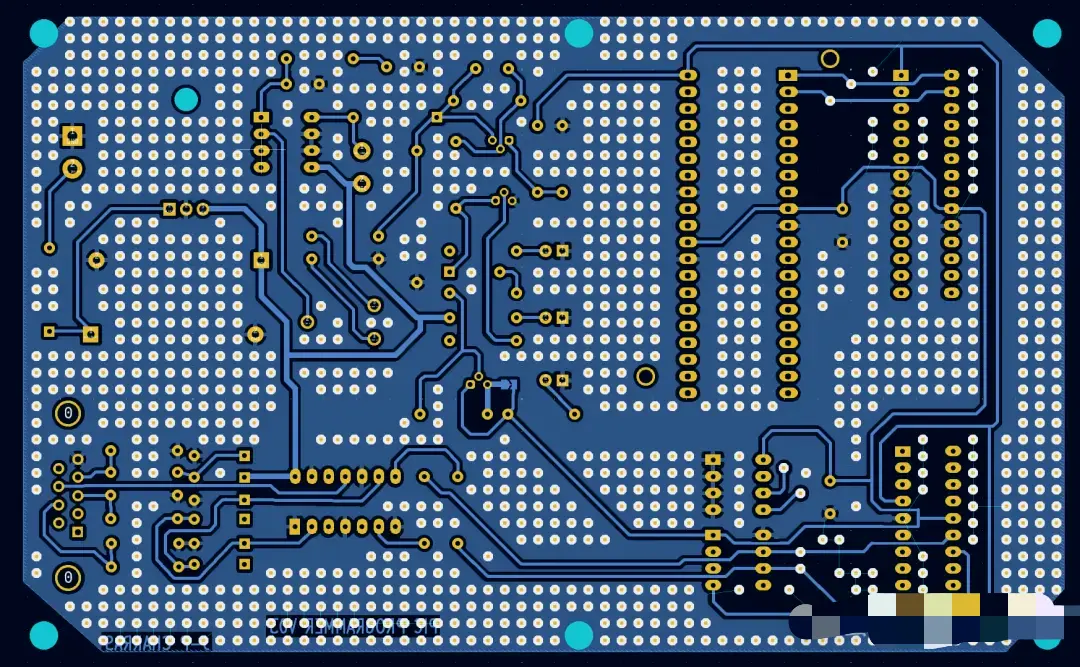
All stitching vias added by the plugin are grouped into a single Group to facilitate quick bulk deletion or editing.
Editing Individual Stitching Vias
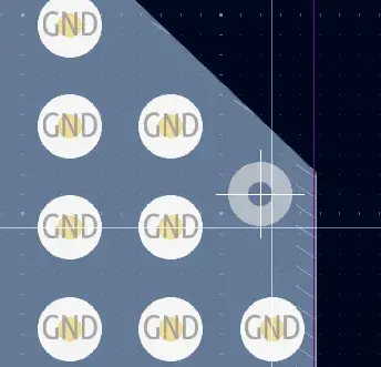
If you need to edit a single stitching via, first select the group of stitching vias, right-click, and choose Enter group. You can then select and move or edit an individual via.
Current Limitations and a Workaround
The current version of the plugin adds stitching vias only within copper zones. It does not yet support placing "guard" vias along a specific track for signal shielding.
A practical workaround is to first place vias along the track manually, then multi-select those vias and use the Properties panel to align or move them as needed and change their net to the desired copper zone (for example, GND). This achieves a guarded trace effect using standard KiCad editing tools.
Design Considerations for Effective Via Stitching
Beyond the mechanics of placing stitching vias, it is important to understand why and where they matter so the result improves electrical and thermal performance rather than just adding drill count. The following guidelines align with common high-speed and power design practices and can be implemented using the plugin's options.
Return Path Continuity
- Whenever a signal changes layers and its return plane changes, the return current must find a path. Place a stitching via close to the signal's transition near the crossing point between reference planes to provide a short, low-impedance return path.
- In mixed-signal or split-plane layouts, stitch across narrow bridges between ground regions so return currents are guided and the loop area remains small.
EMI and Shielding
- Populate stitching vias around the perimeter of the PCB or around copper cutouts and slots. A tight belt of ground stitching vias increases shielding effectiveness and reduces slot antenna effects.
- Along critical routes that require shielding, place guard vias parallel to the trace on both sides when possible. While the plugin currently targets zones, the guarded trace technique described above can be used to create these guard vias.
Thermal Spreading
- Stitching vias can be used as thermal vias to conduct heat from hot copper pours to internal or opposite-side copper. Ensure the via size and annular ring meet your fabricator's capabilities and that solder mask openings are appropriate for the assembly process.
Choosing Grid and Clearance
- Via grid defines density. A tighter grid reduces loop area and improves shielding and thermal conduction but increases drill count and manufacturing cost. Select a grid that balances performance with cost and yield for your board technology.
- Respect your PCB manufacturer's minimum drill size, annular ring, and via-to-copper spacing. Use KiCad's DRC to verify that the chosen via sizes and clearances pass all rules. Because the plugin's clearance control may not be complete in all cases, a DRC pass after placement is essential.
Net Selection and Zone Scope
- Most via stitching is performed on ground (GND) regions, but the plugin allows selecting any copper-zone net. Ensure the chosen net corresponds to a continuous, low-impedance reference or thermal path that you intend to reinforce.
- Use Only under selected Zone to limit placement to a specific zone when a board contains multiple copper regions on the same net. This provides precise control and prevents placing vias in areas where they are not needed.
Layout Practicalities
- Before running the tool, update copper pours so zones reflect the latest outline and clearance shapes.
- Keep stitching vias clear of sensitive component pads, fine-pitch footprints, and test points. The plugin automatically avoids electrical objects, but good placement planning minimizes subsequent edits.
- If your process uses solder mask tenting or via plugging, coordinate mask settings to avoid solder wicking and to meet cleanliness and reliability requirements.
Summary
The kicad-action-scripts Via Stitching tool streamlines a task that otherwise requires repetitive, manual placement. By selecting the appropriate net, via sizes, and grid, and by constraining placement to the zones that matter, you can quickly add a consistent via lattice that improves return path continuity, EMI performance, and thermal conduction. When special guarded traces are needed, the manual via placement and batch property edit workflow offers a workable complement to the plugin.
As with all high-speed and power layout techniques, review DRC after adding stitching vias, verify manufacturability with your PCB fabricator's rules, and focus via density where it delivers the greatest electrical or thermal benefit.