Panelization ties PCB manufacturing economics directly to SMT throughput. A well-engineered panel delivers higher utilization of screen printers, pick-and-place equipment, and reflow lines, while an ill-suited panel can depress line speed, increase handling risk, or even render assembly infeasible. This guide consolidates practical, production-proven techniques for PCB panelization that balance cost, line compatibility, and mechanical robustness from paste print through depanelization.
Panel Size: Make It Fit the Line
Width limitations
Most SMT conveyor systems impose a maximum usable panel width, typically in the 260–300 mm range. When panel width exceeds the line's capability, feeders cannot align properly, conveyor rails cannot grip the panel, and upstream fixtures like printers and AOI cannot reference the board consistently. The result is a drastic reduction in line speed or a forced shift to manual handling—both of which drive cost and variability. Designing your panel within the line's width envelope is the single most effective way to avoid downstream bottlenecks.
Figure 1 | Panel width must comply with SMT conveyor limits, commonly 260–300 mm. Panels that exceed capacity cannot be clamped and transported reliably.
Perimeter rails and outer frame design
- Provide rigid clamping rails. The outer frame must have sufficient stiffness to prevent bow and twist during printing, placement, and reflow. Stiffness helps maintain coplanarity on conveyors and prevents paste smearing or misplacement caused by board flex.
- Do not place V-grooves along clamping edges. V-scoring the rail undermines mechanical integrity and compromises how the panel is gripped by conveyors, printer tooling, and depanel fixtures. Keep the rails continuous and robust.
Beyond gripping, rails also serve as uninterrupted edges for paste printer squeegees and AOI transport. They create clearance for components near the board edge and provide space for barcodes, fiducials, and process markers without intruding on functional circuitry. A well-designed rail system balances strength with minimal material waste to keep panel cost and stack-up consistent.
Component Placement: Orientation and Edge Clearance
Unified component orientation
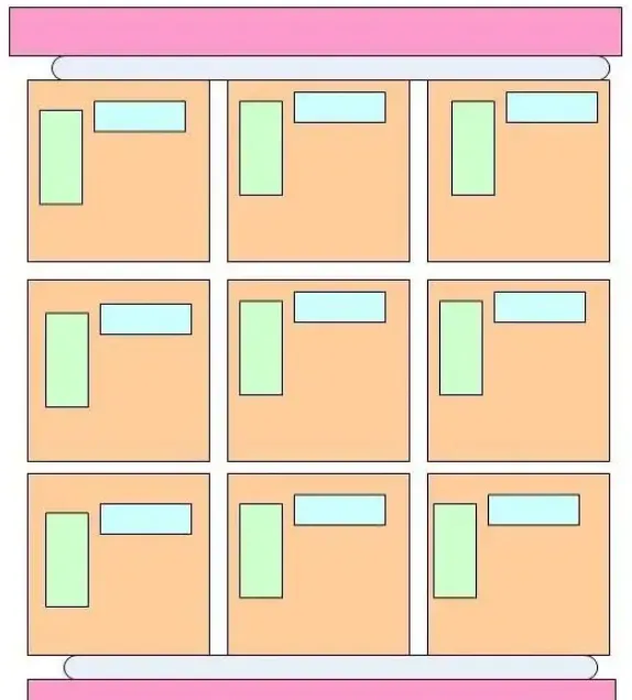
Align all components in a panel with consistent rotation and placement orientation. Mirrored or rotated layouts between sub-boards can misalign centroid data, confuse pick-and-place reference frames, and complicate vision alignment parameters. Uniform orientation reduces programming effort, prevents coordinate errors, and makes feeder optimization more robust across the entire panel.
Edge keepout rules and depaneling space
- Do not let connectors or similar parts protrude beyond the panel edge. Overhang prevents clean depaneling and can collide with fixtures or cutting tools, causing scrap or rework.
- Reserve space between sub-boards for depaneling. Whether using V-scoring or tab-routing, the depanel toolpath needs clearance. Inadequate spacing leads to chipping, rough edges, or stress cracks in the laminate and solder joints.
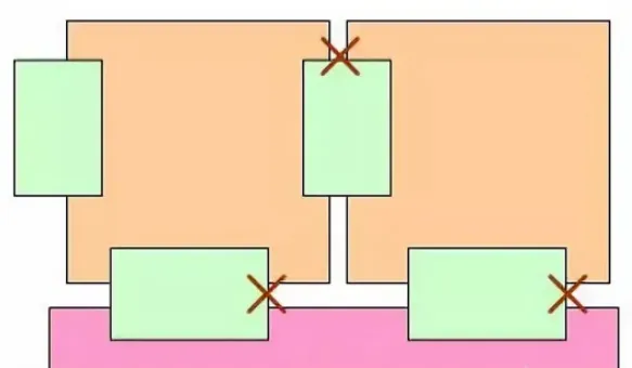
Depanel stress is a critical consideration. Components placed too close to V-score lines or mouse-bite tabs may experience mechanical shock when boards are separated, particularly for brittle packages or large solder joints. Keeping sensitive parts away from depanel lines reduces cracked solder joints, lifted pads, and latent reliability risks.
Registration System: The Backbone of Accuracy
Optical fiducials
- Place at least three optical fiducials per panel. Multiple global fiducials allow vision systems to detect translation, rotation, and slight scale changes, preserving placement accuracy across the panel area.
- Keep a 1.5 mm clear zone around each fiducial free of similar geometries. Avoid silkscreen, copper, solder mask patterns, or vias near fiducials that could confuse machine vision or create false positives.
Global fiducials establish the panel reference frame for SMT, but local fiducials can be placed near fine-pitch devices to fine-tune alignment in high-density areas. Good fiducials include a contrast-enhanced copper pad with a solder mask clearance, offering strong, repeatable recognition by cameras through the full manufacturing stack.
Mechanical tooling holes
- Provide at least three tooling holes per sub-board, with hole diameters between 3 mm and 6 mm. This supports secondary processes such as depaneling fixtures, rework jigs, and end-of-line testing.
- Keep a 1 mm no-go zone around tooling holes for traces and components. Routing close to a tooling hole invites drill breakout issues and can weaken the laminate locally, reducing fixture stability.
Balanced hole placement helps prevent asymmetric stress and improves fixture alignment. When paired with robust rails and fiducials, a comprehensive registration system ensures consistent positional accuracy from paste printing to test and depanelization.
Advanced Techniques: Details That Make or Break a Panel
Direction cues
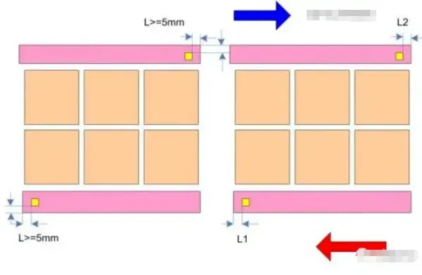
Introduce directional cues along the panel rails using differentiated spacing or notches on orthogonal edges. This makes the panel's flow direction immediately obvious to operators and reduces setup mistakes. Clear direction marking supports correct loading into printers, placement heads, and AOI/AXI equipment, reducing changeover time and preventing mirrored assemblies.
V-score (V-groove) design
- Set score depth to approximately one-third of the board thickness. Controlled residual web thickness ensures the panel holds together during handling yet separates cleanly during depaneling.
- Retain adequate connection bridges. A typical bridge width of around 0.5 mm provides structural continuity without excessive force during break-off.
V-scoring offers faster, cleaner separation on straight edges and is compatible with high-throughput equipment. However, it imposes straight-line constraints and is less suitable for irregular contours. Ensure the score lines do not intersect clamping rails or critical copper features. Consider solder mask clearance and component keepouts along score paths to mitigate cracking or solder joint damage during break-off.
Tab-routing with mouse bites
- Use mouse bites for irregular or curved outlines. Tab-routing allows high geometric freedom when sub-board shapes prohibit straight scoring.
- Select hole diameters in the 0.8–1.0 mm range. Proper hole size supports predictable tab fracture while balancing edge quality and dust generation.
Mouse bites leave small protrusions after break-off that may require sanding or deburring, particularly for cosmetic surfaces or enclosures with tight fits. Space tabs evenly to distribute stress and prevent panel warpage. Keep critical components and fragile features away from tab locations to avoid shock transmission during separation. Coordinate router paths and tab locations with tooling hole and rail placement to maintain rigidity without excess material waste.
Common Issues and Practical Fixes
| Symptom | Root Cause | Corrective Action |
|---|---|---|
| SMT placement offset | Insufficient or obscured fiducials | Add more fiducials and maintain a clean recognition zone around each |
| Difficult depaneling | Connectors protruding beyond the panel edge | Revise placement to keep connectors within the outline and reserve depanel space |
| Panel deformation | Poor clamping rail design | Reinforce rails and avoid V-grooves or slots in gripping areas |
Panelization Golden Rules
- Respect line specs: keep panel width within 260–300 mm to fit common SMT conveyors.
- Design for robust registration: combine global optical fiducials with mechanical tooling holes for reliable alignment.
- Optimize placement: unify component orientation and keep sensitive parts away from edges and depanel paths.
- Plan for downstream processes: reserve sufficient space for depaneling and testing fixtures to reduce scrap and rework.
Applying these practices consistently yields panels that transport reliably, align repeatably, assemble quickly, and separate cleanly. The result is a practical balance of throughput and cost with fewer surprises between design and the factory floor.