Differential signaling is widely used in modern electronic design. Interfaces such as USB, LVDS, and TMDS transmit data over two complementary conductors, commonly referred to as a differential pair. This article explains how KiCad recognizes differential pairs, how to route them in the PCB editor, and how to configure rules and net classes for robust, repeatable results.
How KiCad Recognizes a Differential Pair: Net Naming Rules
KiCad identifies a differential pair as two nets that share a common base name and differ only by a positive/negative suffix. Two suffix styles are supported:
- “+” and “-” suffixes, for example USB+ and USB-.
- “P” and “N” suffixes, for example USB_P and USB_N.
The base name is the shared portion of the net name preceding the suffix. For USB+ and USB-, the base is USB. For USB_P and USB_N, the base is USB_. Note that the underscore is part of the base in this specific naming pattern.
Do not mix suffix styles. For example, USB+ and USB_N do not form a differential pair in KiCad. Differential pairing is determined from the schematic; you must name the nets accordingly in the schematic before you can use the differential pair router in the PCB editor.
The schematic below shows two properly named differential pairs.
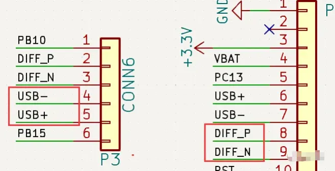
Figure 1 | Two differential pairs identified by P/N or +/- suffixes in the schematic
Once the schematic is annotated and the nets are synchronized to the PCB editor, the differential pair routing command becomes available.
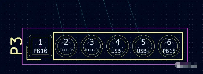
Figure 2 | Differential pair routing command available in the PCB editor
Starting Differential Pair Routing in the PCB Editor
On the right-hand toolbar, long-press the routing tool icon to choose between single-net routing and differential pair routing. The keyboard shortcut for differential-pair mode is 6.
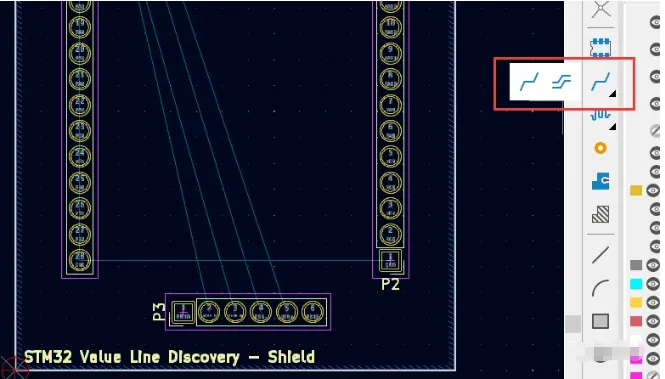
Figure 3 | Selecting the differential pair routing tool (hotkey 6)
Select the intended differential pair and begin routing. The router will track both members of the pair, maintaining the configured spacing as you progress.
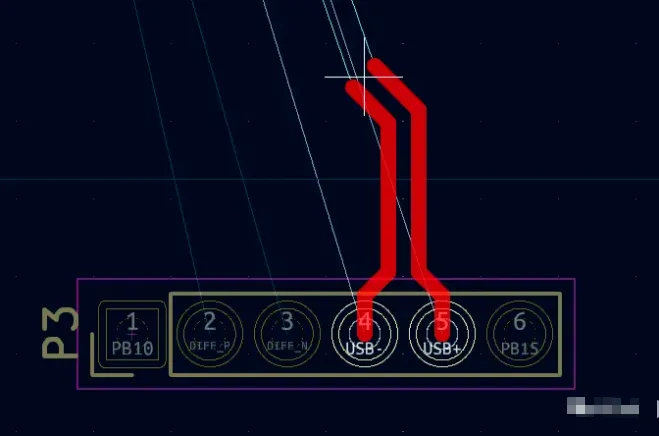
Figure 4 | Beginning differential pair routing on a selected pair
Important: At present, the interactive differential pair router supports starting only from a pin or pad at one end of the pair. Starting in the middle of an already partially routed pair is not supported.
Layer Changes and Via Placement
To transition a differential pair between layers, press V to place a via pair. After placing the vias, continue routing on the new layer. Keep the via geometry and spacing consistent between the two conductors to preserve differential symmetry.
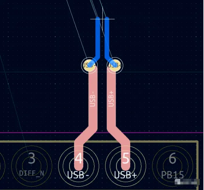
Figure 5 | Using V to place matched vias when changing layers
Setting Differential Pair Constraints
Before routing, define the differential pair constraints in Board Setup. In the Predefined Sizes section, specify common differential pair parameters such as trace width, pair gap (spacing between the two members), and via gap (spacing between the paired vias). This gives the router the clearance and geometry needed to maintain your intended coupling and manufacturability.
During interactive routing, press W or Shift+W to cycle through predefined differential pair sizes. This lets you switch between approved geometries when you encounter tighter areas or different layer stackup requirements.
Net Classes and Scoped Rules
For larger designs, it is convenient to group related differential pairs and apply constraints at the group level. You can define a net class using wildcards or regular expressions that capture a set of P/N nets with a common naming pattern. This allows all members to inherit the same width, gap, and via settings without manually assigning each pair.
Use Custom Rules to further refine constraints for a differential pair net class. For example, you can override the default pair gap for a specific class (such as DP) if those signals require different coupling than the rest of the board. Scoping rules by net class allows you to tailor constraints per interface while keeping the global defaults simple.
Practical Notes and Current Limitations
In the current workflow, differential pairs support straightforward dragging operations, but the push-and-shove behavior is limited. If you adjust one conductor of an already routed pair independently, the spacing will not be preserved automatically, and the pair can become unbalanced. When possible, edit and re-route the pair as a unit so that the router maintains the defined gap.
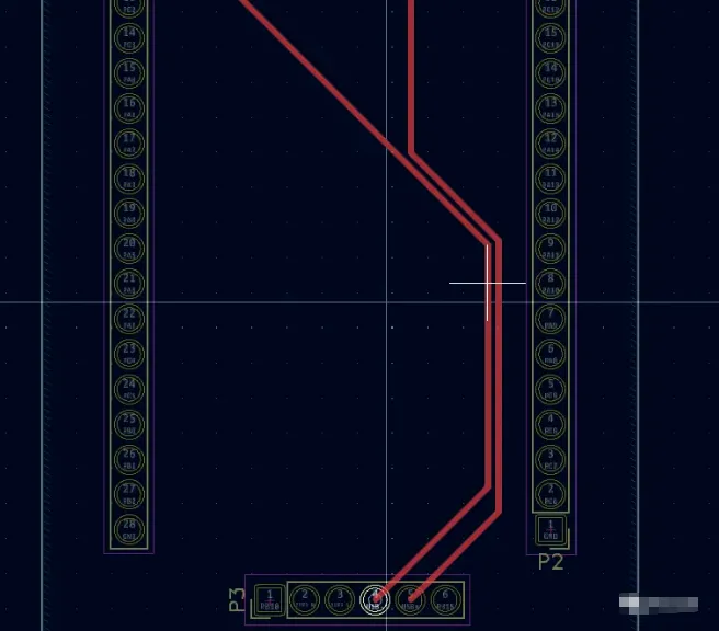
Figure 6 | Changing a single member breaks the fixed pair spacing; re-route the pair to maintain gap
Engineering Considerations When Routing Differential Pairs
Beyond tool operation, the following engineering practices help ensure good signal integrity when implementing differential pairs:
- Maintain consistent spacing. The electrical coupling between the P and N conductors depends on their separation. Large or abrupt spacing changes alter the differential impedance and can introduce reflections. Use the pair gap constraints to enforce a consistent separation, and avoid ad hoc edits to a single conductor.
- Keep geometries symmetrical. When transitioning layers, place the two vias as a matched pair with the same drill and anti-pad dimensions. Keep their centers separated by the configured via gap. Avoid placing one via significantly above or below the other, as asymmetry degrades balance.
- Avoid unnecessary stubs. Tees or unused branches add discontinuities. Plan entry into components to minimize stubs and keep the P/N path lengths similar around bends and connectors.
- Use smooth routing. Favor gradual bends and consistent routing angles on both conductors. Mirrored arcs or matched miter angles help keep electrical length and coupling comparable in the two paths.
- Respect return paths. Differential pairs still reference return currents in nearby planes. Ensure solid, continuous reference planes underneath the pair and avoid crossing slots or gaps that can force return currents to detour.
- Control skew. The two members should arrive at the receiver with minimal timing skew. In layout, match segment counts, bend patterns, and via usage between the conductors to maintain length balance. If you must detour around obstacles, detour both conductors similarly.
- Scope constraints per interface. Different interfaces can require different pair widths and gaps depending on target impedance and stackup. Use net classes and custom rules to keep each interface under the right constraints without overcomplicating the default setup.
Workflow Checklist
- Assign P/N or +/- net names in the schematic using a consistent suffix style for each pair.
- Annotate and update the PCB from the schematic so the PCB editor recognizes the pairs.
- Set differential pair widths, pair gap, and via gap in Board Setup; define predefined sizes for common scenarios.
- Optionally create net classes using wildcard or regex patterns to group related pairs (for example, all DP signals) and apply scoped constraints via Custom Rules.
- Use the differential pair router (hotkey 6) to route pairs as a unit from a pin or pad.
- Drop matched vias with V when changing layers, keeping the via geometry and spacing consistent.
- Switch predefined sizes during routing with W or Shift+W as needed.
- Avoid editing a single conductor independently; re-route the pair to preserve spacing and symmetry.
Following this procedure leverages KiCad's differential pair recognition and routing capabilities while grounding layout decisions in sound signal-integrity practice. Proper net naming, scoped constraints, and disciplined routing workflows help ensure that your USB, LVDS, TMDS, and other differential interfaces achieve the targeted impedance and balanced behavior from schematic through manufacturing.
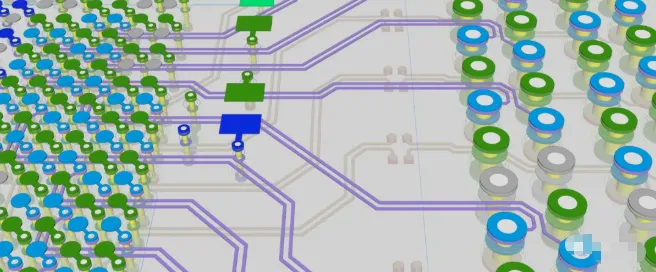
Figure 7 | Overview illustration related to differential pairs in KiCad