A phone that locks up or a PC that stalls is not always a failed IC. Copper thickness on the PCB can be part of the cause. The foil looks minor, but it sets how well the board carries current, spreads heat, and stays mechanically sound.
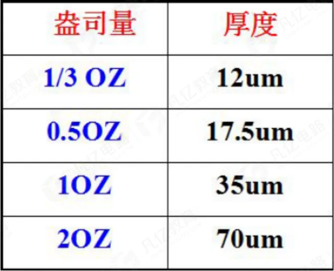
The copper weights used most often are 17.5 μm (0.5 oz), 35 μm (1 oz), and 70 μm (2 oz).
Copper That Is Too Thin Limits Current and Signal
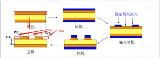
Copper is a good conductor, but a thin layer makes current harder to carry. The signal can weaken along the path, which shows up as a dropped wireless link or a machine that freezes. Thicker is not automatically better. 70 μm (2 oz) copper is generally not the first choice: the board gets heavier and more expensive, resin is more likely to squeeze out in fabrication, and the process is harder to run.
Copper Thickness Also Sets How Well the Board Spreads Heat
As products pack more function, they produce more heat. The copper layer is one of the heat paths. With enough thickness, heat leaves the parts before they shut down on temperature. Unused areas of the board can also be poured with copper to help spread heat.
Copper Thickness Is Part of the Board's Mechanical Strength
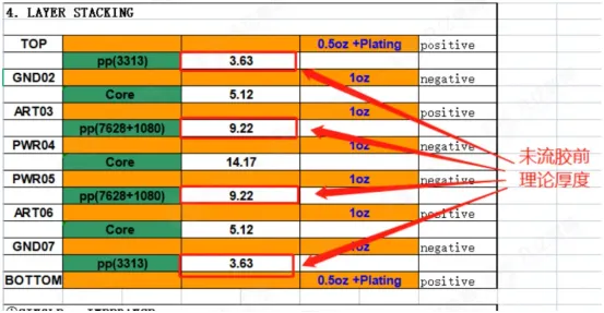
Besides conduction and heat, the copper is part of the board structure. The right thickness makes the PCB stiffer, less likely to bend or crack, and gives a more reliable solder joint, so the assembly lasts longer. Stack-up design and the fabrication flow both have to account for copper weight. If they do not, field failures show up later.
Copper thickness is an unseen control on the product: the right weight keeps current, heat, and mechanics in range. The wrong weight shows up as repeated small failures.