Introduction
Copper weight (expressed as oz/ft²) is one of the most frequently misunderstood specifications in PCB design. It directly affects current capacity, thermal performance, trace resistance, impedance, mechanical strength, and PCB manufacturing cost. This article explains exactly what copper weight means, where it matters most in real designs, and how thickness requirements are defined by IPC standards.
What “Copper Weight” Actually Means
- 1 oz copper = 34.8 µm (1.37 mil) thick foil before processing
- 2 oz copper = 69.6 µm (2.74 mil)
- 0.5 oz copper = 17.4 µm (0.68 mil)
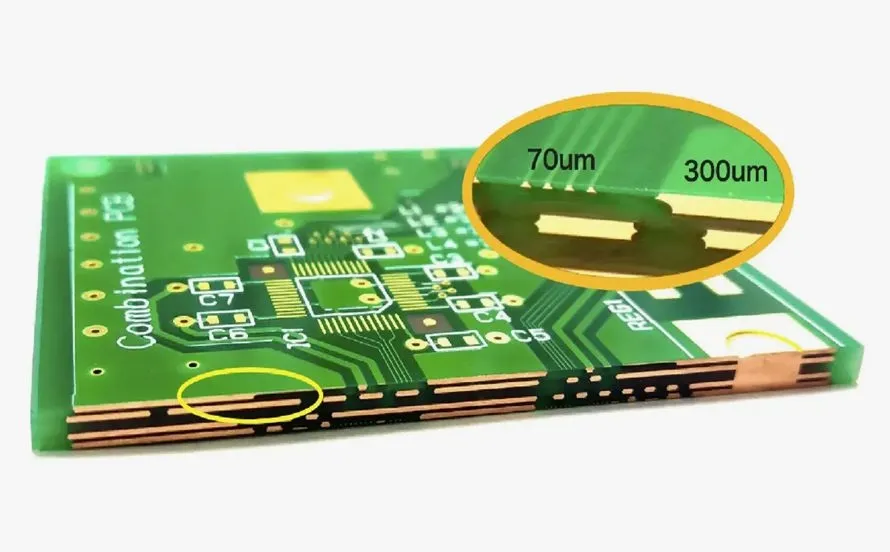
These are starting (base) foil thicknesses.
On outer layers, finished thickness = base foil + plating (usually +20–30 µm).
On inner layers, finished thickness = base foil only (no additional plating).
Where Copper Weight Matters Most
| Design Area | Why Copper Weight Is Critical | Recommended Weight |
|---|---|---|
| Power supply traces | Lower resistance → less voltage drop and heat | 2–3 oz |
| LED boards, motor drivers | Heat spreading and current handling | 2–4 oz |
| High-speed controlled impedance | Precise thickness needed for exact 50 Ω or 100 Ω | 0.5–1 oz (outer) |
| Fine-pitch BGA fanout | Thinner copper allows narrower traces and spacing | 0.5 oz inner |
| Battery management | Minimize IR drop on high-current paths | 2–3 oz |
| RF and microwave | Skin effect and lower loss with thicker copper | 1–2 oz |
| Mechanical strength | Thicker copper survives vibration and flexing | 2+ oz |
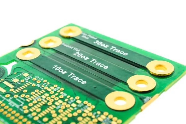
Relation Between Copper Weight, Trace Width, and Current
Example using IPC-2221B external trace, 10 °C rise:
| Copper Weight | Trace Width for 3 A | Trace Width for 6 A |
|---|---|---|
| 1 oz | 2.20 mm | 5.10 mm |
| 2 oz | 0.95 mm | 2.30 mm |
| 3 oz | 0.60 mm | 1.45 mm |
Doubling copper weight roughly halves the required trace width for the same current and temperature rise.
Does “Standard Thickness” Always Matter?
No – only where performance demands it.
| Situation | Standard 1 oz OK? | Better Choice |
|---|---|---|
| Simple Arduino shield | Yes | 1 oz |
| 4–8 layer HDI with 0.4 mm BGA | No | 0.5 oz inner |
| 48 V / 20 A DC-DC converter | No | 2–3 oz outer |
| USB/Ethernet impedance board | Yes (if calculated correctly) | 1 oz outer |
IPC-6012E Minimum Finished Thickness Requirements
| Location | Class 2 Minimum | Class 3 Minimum |
|---|---|---|
| Plated-through hole wall | 20 µm average | 25 µm average |
| External finished trace | Base + plating | Base + plating |
| Inner-layer foil (finished) | No minimum (design-driven) | No minimum |
Never assume “1 oz” gives 35 µm in the holes – typical finished hole copper with 1 oz starting foil is only 23–28 µm.
Practical Guidelines for Designers
- Always specify starting copper weight per layer in the fabrication drawing
- For Class 3 or high-reliability, start with 1 oz outer foil + request 25 µm average hole plating
- Use 2 oz or heavier when trace width would exceed 3–4 mm at 1 oz
- Use 0.5 oz inner layers when trace/space drops below 0.10/0.10 mm
- Remember impedance calculators need finished thickness, not just “1 oz”
Conclusion
Copper weight is not a “one-size-fits-all” specification across different types of PCBs. It must be chosen deliberately based on current capacity, thermal dissipation, impedance control, and mechanical reliability. Understanding the difference between starting foil and finished plating thickness, and applying IPC-2221B and IPC-6012E correctly, prevents overheating, excessive voltage drop, impedance errors, and costly re-spins.
FAQs
Q1: Is 1 oz copper always 35 µm thick?
A1: Only the starting base foil. Finished outer traces are 55–65 µm after plating; hole walls are typically 23–28 µm.
Q2: Can I get exactly 35 µm in plated holes with 1 oz copper?
A2: No. To guarantee ≥ 25 µm average hole copper (Class 3), fabricators start with 1 oz foil plus extra panel plating time.
Q3: When should I switch to 2 oz copper?
A3: When your widest power trace at 1 oz would exceed ~4 mm, or when voltage drop and heat become design constraints.
Q4: Does thinner copper reduce impedance for the same trace width?
A4: Yes. A 50 Ω trace on 0.5 oz copper is narrower than on 1 oz copper for the same stack-up.
References
IPC-2221B — Generic Standard on Printed Board Design. IPC, 2015.
IPC-6012E — Qualification and Performance Specification for Rigid Printed Boards. IPC, 2017.
IPC-TM-650 2.3.28 — Plating Thickness Measurement. IPC, 2016.
IPC-TM-650 2.2.12 — Determination of Copper Foil Thickness. IPC, 2010.