A circuit board must pass manufacturability, process capability, signal integrity, EMC, and other gates on the way from the design drawing to volume production. This article organizes 13 common but critical PCB design concepts, sorts the design logic, and strengthens engineering judgment.
1. FR-4 Laminate: The Base That Carries the Signal
FR-4 is the most commonly used PCB base material. It is a copper-clad laminate made by pressing glass cloth with epoxy resin. Heat resistance is measured by Tg (glass transition temperature).

- Low-Tg material (Tg ≈ 130 °C): used for conventional applications
- Mid-Tg material (Tg > 150 °C): suitable for circuits of moderate complexity
- High-Tg material (Tg ≥ 170 °C): recommended for high-temperature soldering, lead-free processes, and high-reliability uses such as automotive and communications
High-Tg material is not only more heat-resistant. Moisture resistance and chemical resistance also improve significantly, which helps keep multilayer boards dimensionally stable over long-term operation.
2. Impedance Matching: Protecting High-Speed Routing

In high-speed digital circuits such as DDR, USB, and PCIe, a signal without accurate impedance matching can produce reflection, crosstalk, and related problems. Common controlled-impedance targets include:
- Differential impedance: 100 Ω / 90 Ω
- Single-ended impedance: 50 Ω
How is the match designed? Precise simulation must combine stackup, trace width and spacing, reference planes, and dielectric constant.
3. Surface Finish: What Decides Solder Quality and Life
Five common surface finishes:
| Process | Advantages | Disadvantages | Typical use |
|---|---|---|---|
| HASL | Low cost, mature process | Uneven surface, oxidizes quickly | High-volume consumer products |
| Immersion tin | Good planarity | Oxidizes and darkens easily | Communications products |
| ENIG | Good solderability and contact | Higher cost | High-frequency boards / BGA |
| Electrolytic gold | High hardness and wear resistance | Poor solderability | Gold fingers, keys |
| OSP | Very low cost | Oxidizes easily, lower reliability | Fast prototypes |
For high-frequency impedance control, ENIG or immersion tin is strongly recommended. HASL should not be used on BGA boards.
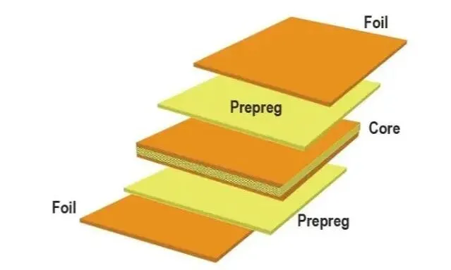
4. Core and Prepreg: The Materials That Set Thickness, Stackup, and Electrical Performance
Core plus PP (prepreg) determines the structure and stability of a multilayer board. Thickness, resin flow, and electrical constants must be coordinated with stackup simulation.
- Core: a rigid board already laminated with copper on both sides
- PP: semi-cured resin used to bond layers
Use a balanced mix to avoid process problems such as warpage during lamination, voids, and copper peel.
5. Differential Pairs: Signal Integrity Needs Routing Symmetry

Differential signals are used for high-speed data such as LVDS, USB, and PCIe. They must meet:
- Equal length, equal width, and equal spacing
- A consistent reference ground
- No discontinuity in the reference plane
Asymmetry in a differential pair directly affects clock skew and crosstalk. It must be planned during placement.
6. Signal Integrity (SI): The Core of High-Speed PCB Design
Five major factors that affect signal integrity:
- Reflection (impedance mismatch)
- Crosstalk (traces too close)
- Ground bounce (ground-return interference when multiple devices switch at the same time)
- Improper filter design
- Unreasonable PCB structure
SI problems often lead to system failure, frequent resets, and data errors.
7. Signal Reflection: Do Not Send the Signal Back Along the Same Path

Signal reflection can cause:
- Overshoot
- Undershoot
- Ringing
- Stair-step waveforms
To control reflection, impedance matching is not enough. Proper termination (source end and load end) is also needed, and reference-plane breaks must be avoided.
8. Crosstalk: Noise Coupling Between Signal Lines
Tightly packed high-speed traces with no ground reference can produce severe crosstalk, especially when DDR or high-speed buses run side by side.
- Capacitive coupling → current crosstalk
- Inductive coupling → voltage crosstalk
Countermeasures: add ground-guard traces, use reasonable spacing, and control routing direction.
9. Internal Power Planes: A Tool for Stable Supply and Interference Control
Power and ground must be designed as large-area planes, with reasonable partitioning and dense via placement, to avoid floating islands and broken power loops.
10. Blind and Buried Vias: A Key Method for High-Density Boards
Figure 9 | Layer structure of blind vias and buried vias
- 1-step blind via: L2–TOP
- 2-step blind via: L3–TOP
- Buried via: interconnection between L3 and L6
HDI boards use large numbers of blind and buried vias, which can raise space utilization significantly, but they increase cost and process requirements.
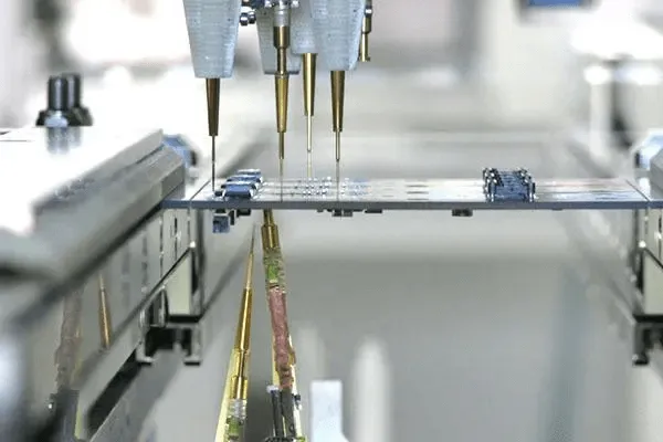
11. Test Points: A Safeguard Reserved for Production Debug

They are used for functional test, in-system programming, and debug location. BGA regions must be handled with flying probe or boundary scan.
12. Fiducials: What Protects SMT Placement Accuracy
Fiducials are used for SMT placement location. Recommended practice:
- A 1 mm circle is the most common size
- Leave a solder-mask opening around the mark
- Place three fiducials on the board in a symmetric arrangement, with a consistent copper background
13. PTH and NPTH Holes: Carriers for Connection and Fastening
- PTH (plated through-hole): used for electrical connection
- NPTH (non-plated hole): used for mechanical location, screw mounting, and similar functions
Hole attributes must be marked accurately in the fabrication files to avoid rework.
Conclusion: Quality PCB Design Comes from Controlling the Critical Details
PCB work is not simply drawing. It is a system task that must balance electrical performance, process feasibility, production cost, and later maintenance. Understanding the design logic and engineering meaning behind each term is the starting point for becoming a professional PCB engineer.
SEO Title: 13 PCB Design Fundamentals from FR-4 to Fiducials Meta Description: Thirteen PCB fundamentals covering FR-4, impedance, surface finish, stackup, SI, vias, test points, and fiducials, from layout through manufacturability.