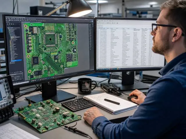
Can AI automatically route a multi-layer PCB? On moderately dense boards with clear design rules it can finish most of the nets and produce usable candidates in far less time than a full manual route. Tools such as DeepPCB and Quilter already demonstrate high completion rates on 4- to 6-layer designs when the placement and constraints are well defined. The output still needs engineering review for return paths, impedance continuity, and manufacturing constraints. AI reduces repetitive work; it does not remove the need to verify that the finished geometry preserves signal integrity and can actually be built.
Most of the value appears when the board has hundreds of nets and several layer transitions. The remaining work is almost always on the critical nets and the plane discontinuities the tool did not fully see.
What Current AI Routing Actually Does
AI routers take the netlist, component placement, layer stackup, and design rules, then search for paths that satisfy clearances, widths, and via constraints. Some systems use reinforcement learning trained on completed boards and physics checks for return paths or basic coupling. Others act as guided routers that complete unfinished nets while leaving designer-routed critical sections untouched. On a 6-layer board with a few hundred connections the tools can reach 95 % or higher completion in minutes to a couple of hours. Traditional grid-based autorouters often leave more cleanup because they optimize only for connectivity.
The result is a routed board, not a finished design. You still inspect every high-speed net, every plane split, and every via transition.

Layer Assignment and Via Reduction
Some AI systems propose layer assignments based on net density and declared signal classes. They prefer to keep high-speed nets on layers that already have continuous ground references and to minimize layer hops on matched groups. Via count is one of the clearer improvements. On comparable boards the better AI routers have produced noticeably fewer vias than classic autorouters while still completing the nets. That matters on multilayer boards because every via is a potential stub and a return-path jump.
The tool still needs the stackup and the priority list up front. If the high-speed nets are not marked, or if the ground planes are already fragmented, the AI will route over the discontinuities it was not told to avoid.
Help with Density and Repetitive Connections
Escape routing from dense BGAs and large parallel buses is where the time savings show up. The AI can explore many short paths and layer transitions that a designer would try only once or twice. On boards with several hundred nets the difference between manual completion and AI-assisted completion is often measured in days rather than hours. Differential pairs and length-matched groups can be held together if the rules are explicit. The tool is less reliable when the constraints conflict—tight impedance, minimum via stubs, and limited channels at the same time.

Signal Integrity Assistance and Its Limits
Physics-aware AI can penalize routes that cross plane splits or that lack nearby stitch vias. It can also keep differential pairs on the same layer with consistent spacing when those rules are supplied. That is useful. It is not the same as full SI simulation. Most current tools do not run eye-diagram or crosstalk analysis inside the routing loop. They optimize for geometric and basic electromagnetic constraints that were part of the training or the rule set. Unusual edge rates, specific EMI limits, or interactions between multiple high-speed interfaces still need separate simulation and review.
A continuous ground under a critical net is still the designer's responsibility to define and to verify after the AI finishes.
DFM and Manufacturing Constraint Checks
AI can flag or avoid obvious manufacturing issues when those limits are loaded as rules: minimum trace width and spacing, via size and annular ring, copper balance, and basic clearances to the board edge. Some systems generate multiple candidates so the designer can compare via count, length, and copper distribution. They do not know the specific fabricator's process window, etch compensation, or impedance coupon correlation unless those details are supplied. Copper density that looks balanced in the tool can still warp after lamination if the real stackup and resin flow differ from the model.
Where AI Still Needs an Engineer
Complex electrical constraints that were not in the training set or the rule file produce routes that pass DRC but fail in the lab. Impedance control depends on the finished dielectric thickness and etch undercut; the AI uses the values you give it. EMI/EMC performance, thermal hotspots, mechanical stress on vias, and mixed-signal isolation decisions remain outside most current models. Novel topologies or unusual stackups degrade the result because the systems interpolate from prior examples. On multilayer boards the combination of via stubs, reference-plane changes, and length matching is still easier for an experienced designer to resolve on the critical nets than for the AI to get right on the first pass.

Practical Workflow with AI Assistance
Lock the schematic and place the critical components first. Define the stackup, net classes, impedance targets, differential pairs, and length-matching groups. Load the fabricator's minimums and the preferred layer assignments. Let the AI complete the bulk of the routing or generate candidates. Then review every clock, differential pair, and power net for continuous reference, stitch vias at layer changes, and acceptable spacing. Run SI simulation on the critical interfaces and a DFM check against the actual process. Adjust the rules and re-run if the first candidates create too many discontinuities. The AI handles the volume; the engineer still owns the constraints and the final verification.
What Must Be Clear Before You Ask AI to Route
The design rules, net priorities, layer constraints, impedance targets, and manufacturing limits have to be explicit. High-speed nets need continuous ground references declared. Differential pairs and matched groups need their skew and spacing rules set. Plane splits and keep-out regions must be visible to the tool. Without those inputs the question "can AI automatically route a multi-layer PCB" has a technical answer—yes, it can connect most nets—but the practical answer remains no, not to a state you can release without review. AI accelerates the middle of the layout. The stackup, the return paths, and the final judgment stay with the engineer.