A DP interface is DisplayPort, the display interface published by VESA. DisplayPort carries video and also supports high-definition audio, together with higher resolution and refresh rate. The DP 1.4 port specification is based on DP 1.3. The lane width is unchanged. Display Stream Compression, forward error correction, and high-dynamic-range packets are added.
-
Add ground vias in the BGA region at the locations shown in Figure 1-1 (a). Apply ground fencing as shown in Figure 1-1 (b). L is the ground-via pitch on the fence. D is the air gap between the fence and the signal. D ≥ 4 × W is recommended.
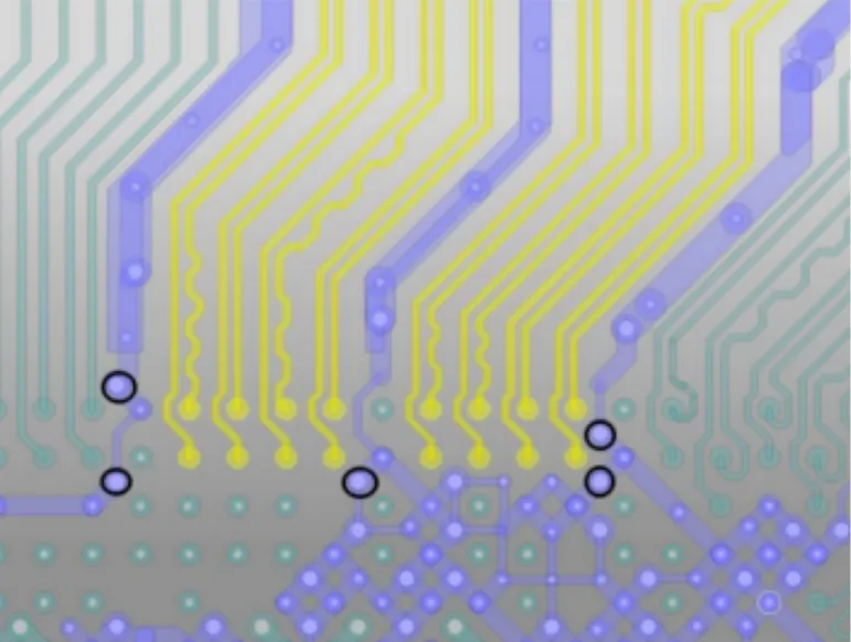
Figure 1-1 (a) | DP BGA region fan-out
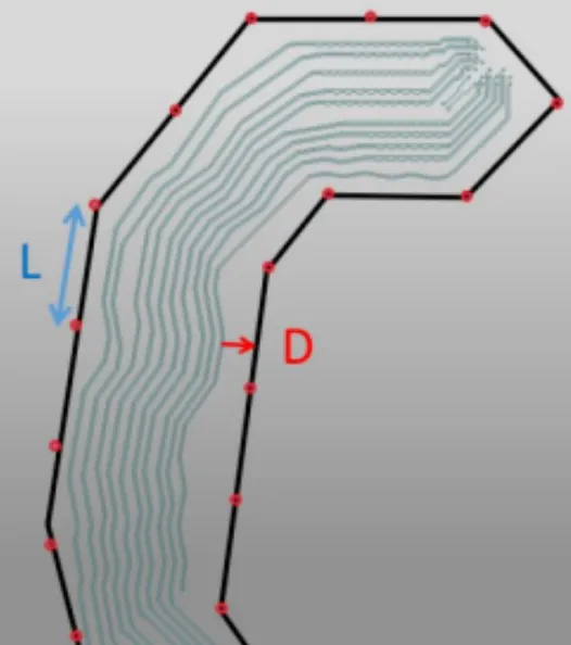
Figure 1-1 (b) | Recommended ground fencing
-
Hold intra-pair length mismatch to 6 mil. Apply length matching as shown in Figure 1-2.
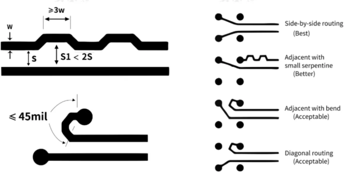
Figure 1-2 | Intra-pair length-matching rules
Note: When the DP connector operates at ≥ 8 Gbps, follow the connector recommendations below.
- Exit traces from the center of the connector footprint. If one side of a high-speed signal in the connector is not next to a GND pin, add a GND via beside that signal in the layout.
- If the interface data rate is ≥ 8 Gbps, the connector must meet the matching standard (for example HDMI 2.1, DP 1.4, or PCI Express 3.0). Recommended connector vendors include Molex, Amphenol, and HRS.
- Void one or two ground planes under the interface, depending on the connector. If L2 under the connector pads is voided, the reference must skip a layer and L3 must be the ground reference. If both L2 and L3 ground references are voided, L4 must be a ground plane and serve as the skip-layer reference. Void size must be set from the connector part number and confirmed by simulation on the actual stack-up after that stack is locked for HDMI / DP 100 Ω.
- Place two ground vias on each connector ground pad, as close to the pad as possible.
Reference void sizes based on an EVB first-order HDI stack-up are given below.
Recommended connector routing:
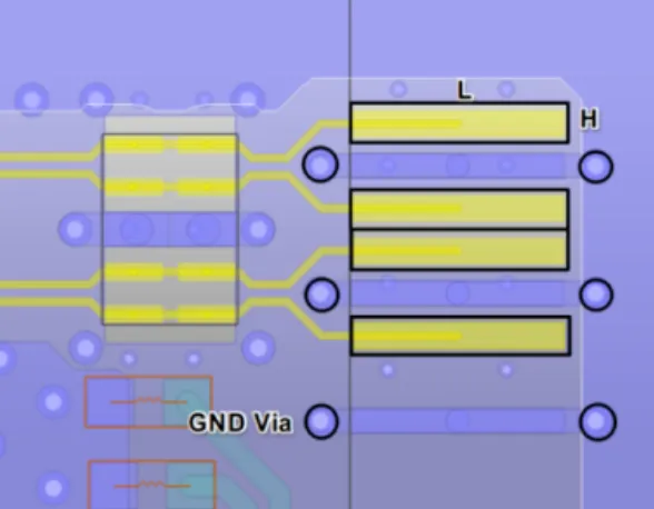
Figure 1-3 | DP connector routing