 03:41
03:41
BGA Design
Ball Grid Array (BGA) design represents a cornerstone of modern printed circuit board (PCB) engineering, enabling high-density component placement and enhanced performance in compact electronic devices. This tag encompasses a range of articles focused on the intricacies of BGA implementation, from initial layout considerations to advanced manufacturing techniques. For engineers and designers searching for BGA Design guidance, these resources address common challenges such as signal integrity, thermal dissipation, and reliable soldering processes, which are critical in applications like smartphones, servers, and automotive electronics. Understanding BGA Design begins with recognizing its advantages over traditional packaging methods, including reduced footprint and improved electrical connectivity through an array of solder balls. However, it demands precise attention to detail to avoid issues like voiding during reflow or misalignment in assembly. Practical insights covered here include best practices for via placement, escape routing strategies, and layer stackup optimization to minimize crosstalk and ensure manufacturability. For instance, incorporating blind and buried vias can streamline high-pin-count BGA layouts, while thermal vias under the package help manage heat in power-intensive designs. These approaches not only enhance reliability but also reduce time-to-market by aligning with industry standards like IPC-7351 for land pattern design. Professionals tackling BGA Design often seek ways to balance cost and performance, such as selecting appropriate substrate materials or simulating electromagnetic interference early in the process. The articles under this tag provide step-by-step guidance on tools like CAD software for fanout patterns and validation methods using X-ray inspection. By delving into these topics, readers can apply proven methodologies to their projects, whether prototyping a new IoT device or refining an existing high-speed PCB. Browsing the linked posts offers deeper dives into specific case studies and troubleshooting tips, helping you refine your skills in this essential area of electronics design.
Video Guide

Technical Articles
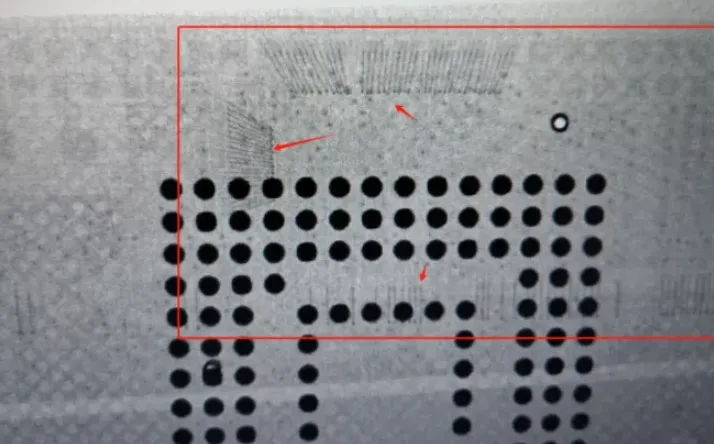
X-Ray Inspection of eMMC BGA: Solder Ball Assessment and an Unexpected Finding
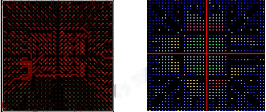
PCB Via Fanout Details That Are Easy to Miss
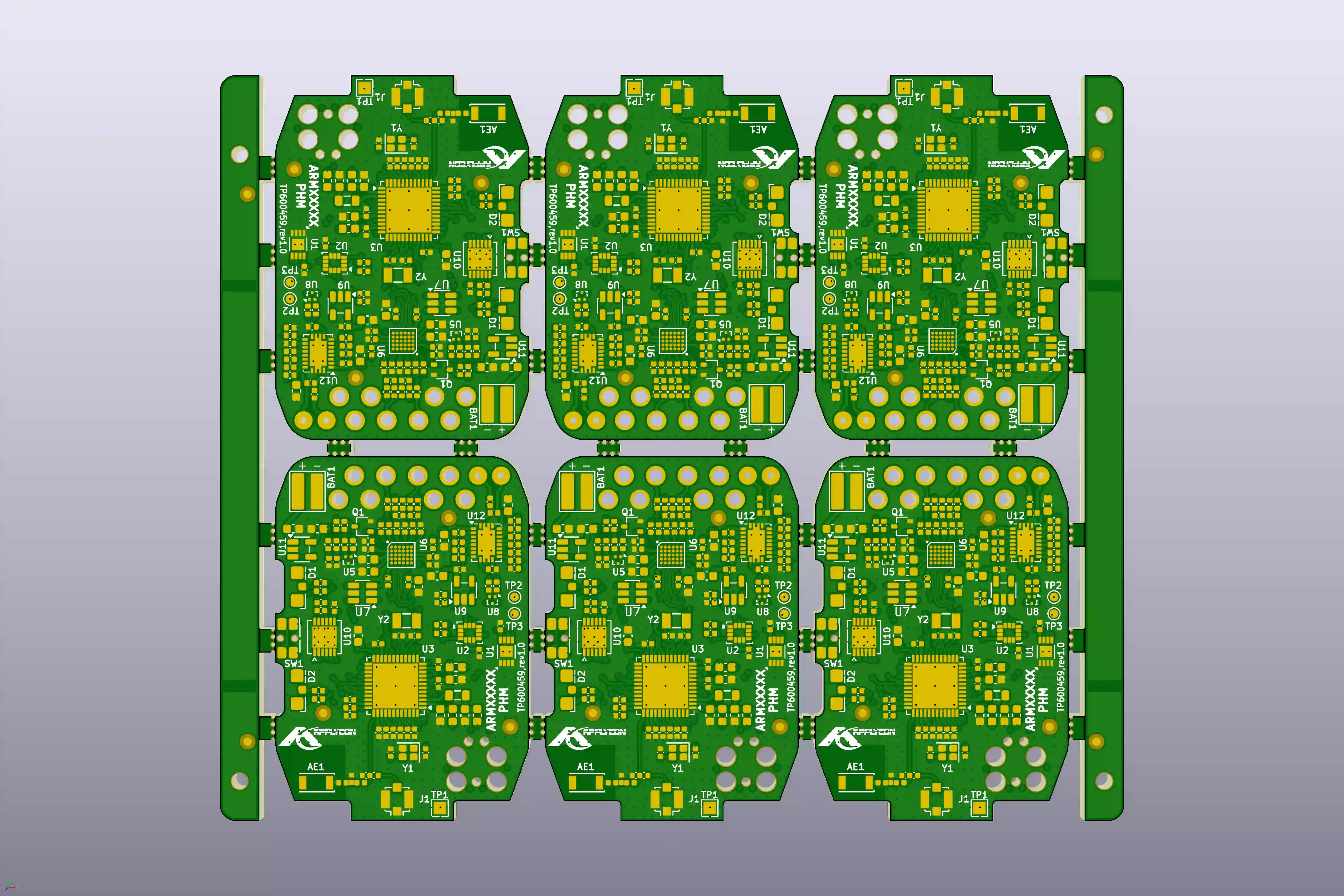
How to Avoid Common Solder Mask & Stackup Issues in 6-Layer HDI PCBs
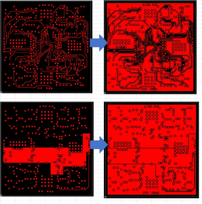
How to Prevent Lamination Failures in 8-Layer HDI PCBs
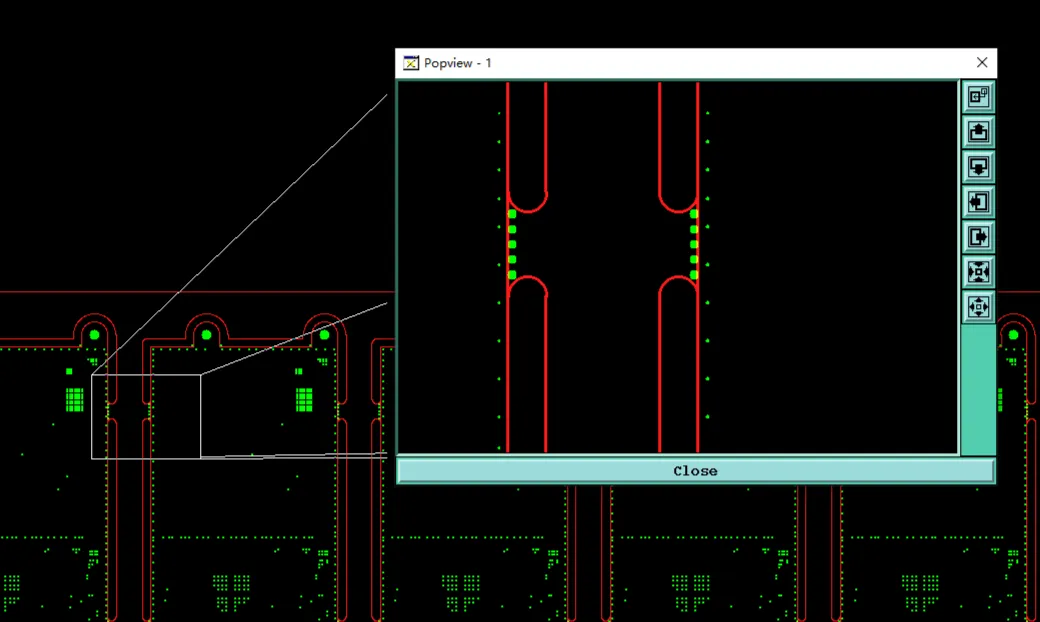
How to Prevent Solder Mask Bridge Failure and NSMD BGA Issues in 8-Layer PCB
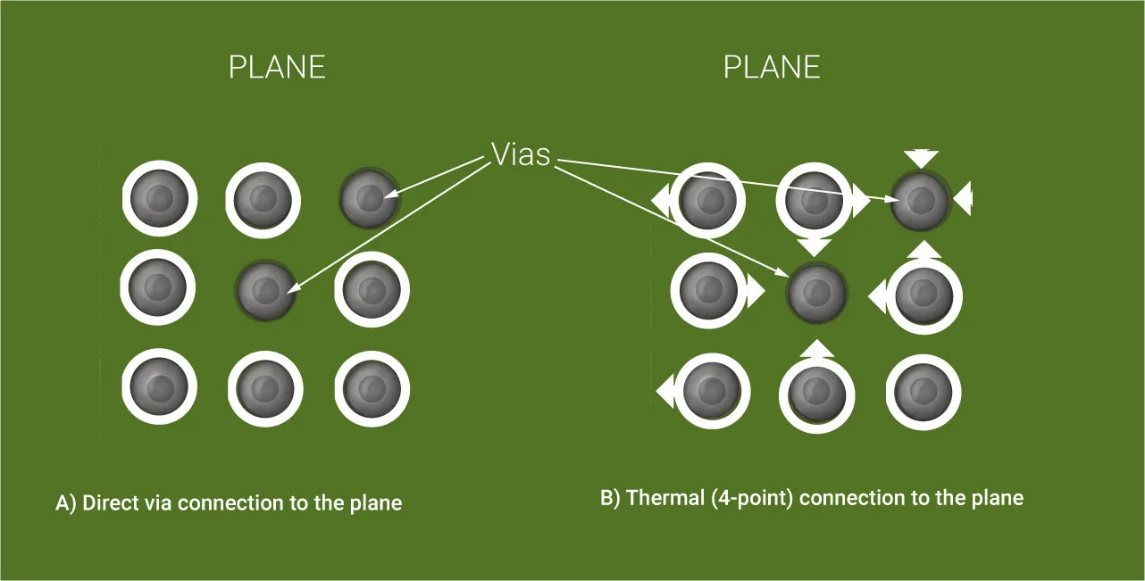
BGA Breakout Cost Optimization: Balancing Performance and Manufacturing Costs
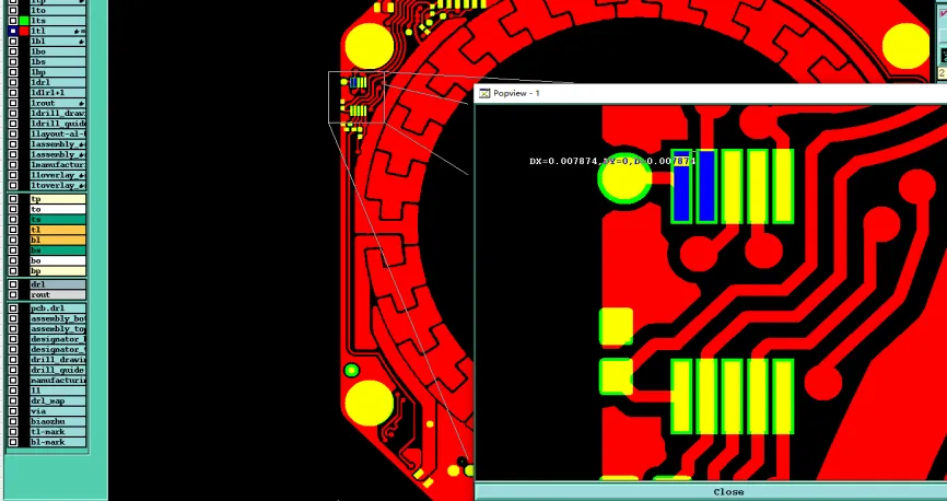
2-Layer High-TG FR-4 PCB Engineering Case: Copper Thickness vs. Fine Line Conflict and Solder Mask Bridge Challenges in BGA Region
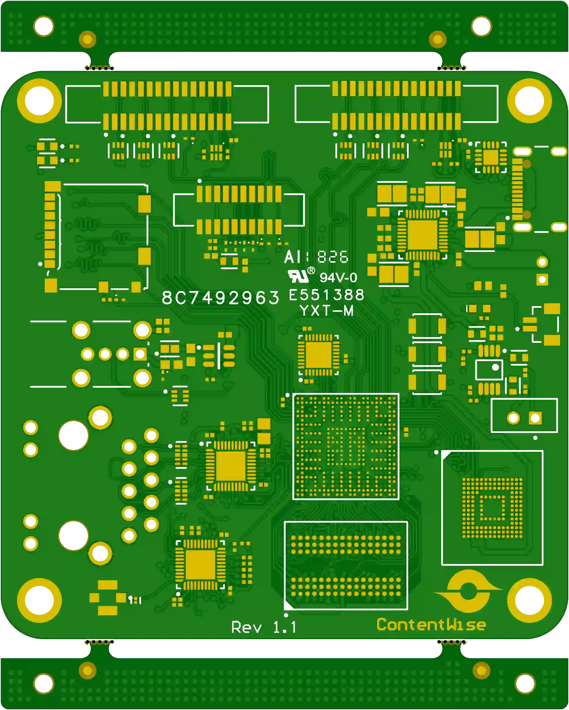
8-Layer Impedance-Controlled PCB Engineering Case: Stackup Mismatch, Missing Reference Traces & BGA Solder Mask Risks
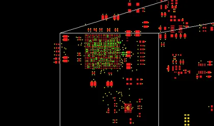
6-Layer FR-4 PCB Engineering Case: BGA Solder Mask Conflicts, Silkscreen Overlap, and Custom Labeling Challenges in CAM Review
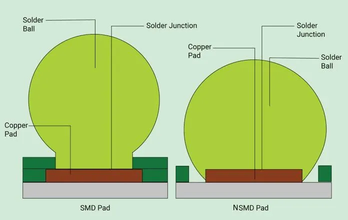
SMD Pad vs NSMD Pad for HDI BGA: Which Is Better?
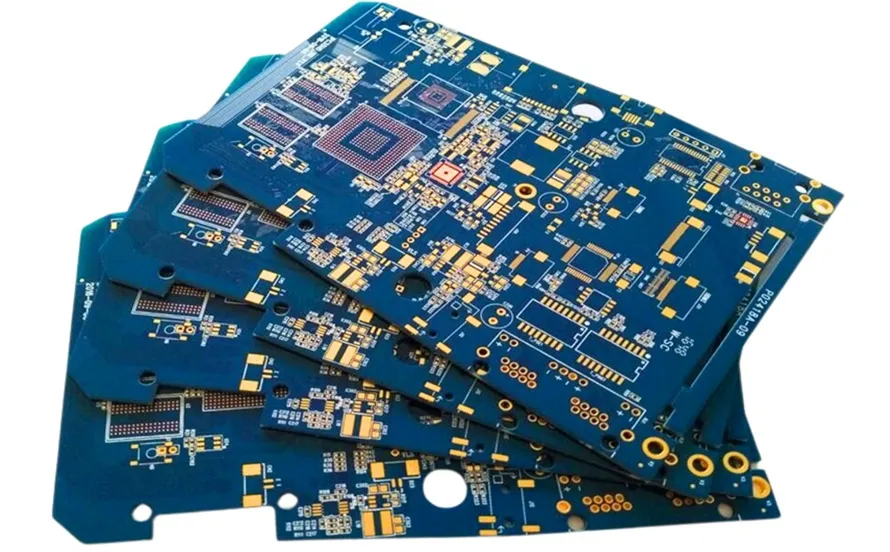
Common Via-in-Pad Design Mistakes in HDI PCB

HDI BGA Fanout Design Mistakes That Cause Assembly Issues
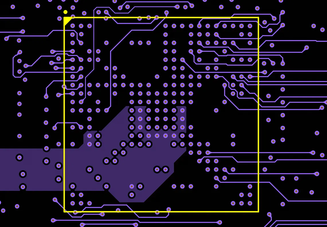
Basics of routing with BGA packages
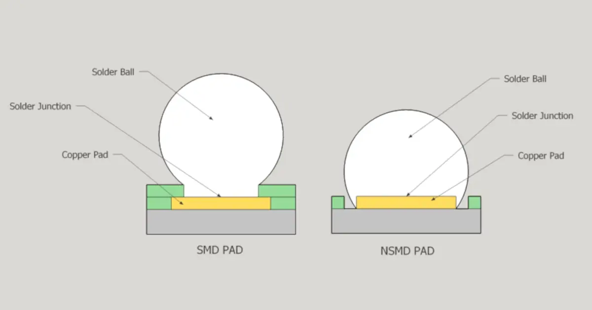
Fanout and routing: How to connect BGA packages to the rest of the PCB
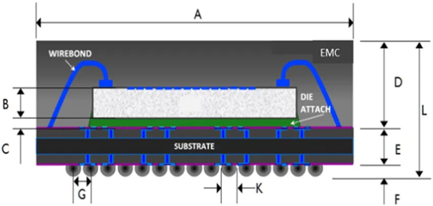
A Comprehensive Guide to BGA Assembly and Inspection
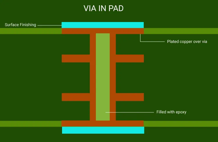
Via-in-Pad Without Fanout Advantages and Disadvantages
Optimizing BGA Assembly: The Critical Role of Solder Mask Thickness

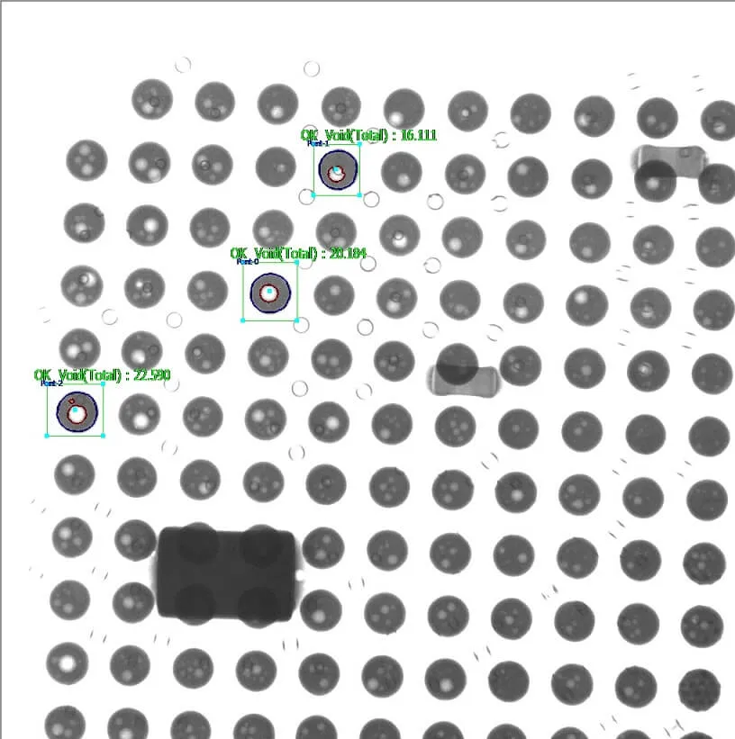
Uncovering Hidden PCB Defects: A Guide to BGA X-Ray Inspection
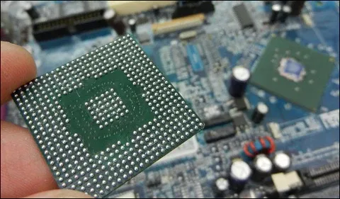
Navigating BGA Escape Routing: Essential Techniques for High-Density PCBs