In this real-world CAM engineering review for a 2-layer 1.6mm FR-4 TG170 board (87×87mm), our team encountered several critical DFM issues centered around outer layer 2oz copper thickness compatibility with tight 6-7.87mil spacing and solder mask bridge feasibility in dense BGA areas. What started as a straightforward high-TG order quickly required multiple engineering clarifications to prevent production risks.
Introduction
This case study examines a standard 2-layer PCB order intended for electronic applications requiring elevated thermal performance. The customer specified High TG material (TG ≥ 170°C), 1oz/2oz copper, ENIG surface finish, and 100% flying probe testing for 200 pieces. Such boards are common in industrial controls and power-related devices where thermal reliability matters.
However, during our standard CAM engineering review, discrepancies between the provided Gerber/ODB data and our manufacturing capabilities surfaced. The primary challenges involved finished copper thickness conflicts with minimum line spacing and insufficient pad-to-pad clearance for reliable solder mask bridges under 2oz copper weight. These are classic manufacturability gaps that frequently arise when design rules are based on lighter copper assumptions.
Our CAM team raised targeted Engineering Questions (EQs) to align design intent with production realities. This review process is essential because proceeding without clarification often leads to scrap, rework, or field failures. In this article, I will walk through the specific issues identified, the risks involved, and how we resolved them — from a senior CAM engineer's perspective with over 15 years in PCB fabrication.
Order Overview
The PCB is a 2-layer board ( #FR4-20260126-052 ) using FR-4 TG170 material (KB-6167F equivalent), sized 87mm × 87mm with 1.6mm finished thickness. Outer copper is specified as 2oz, inner (effectively base) at 1oz. Minimum hole size is 0.25mm, with line width/space at 6mil. Surface finish is ENIG (immersion gold), solder mask is cold white on both sides, and silkscreen is black. The order is single-piece shipment (no panelization beyond 1x1), mechanical routing, no V-cut, and includes full electrical testing.
Customer notes emphasized High TG material compliance. Delivery target was 11 days for 200 pieces. While the stackup and material selection were generally manufacturable, the combination of 2oz finished copper with sub-8mil spacing in dense areas created immediate flags in our DFM analysis. Panel utilization was straightforward, but trace/pad geometry required close scrutiny.
Main Engineering Questions Found During CAM Review
File & Manufacturing Data Issues
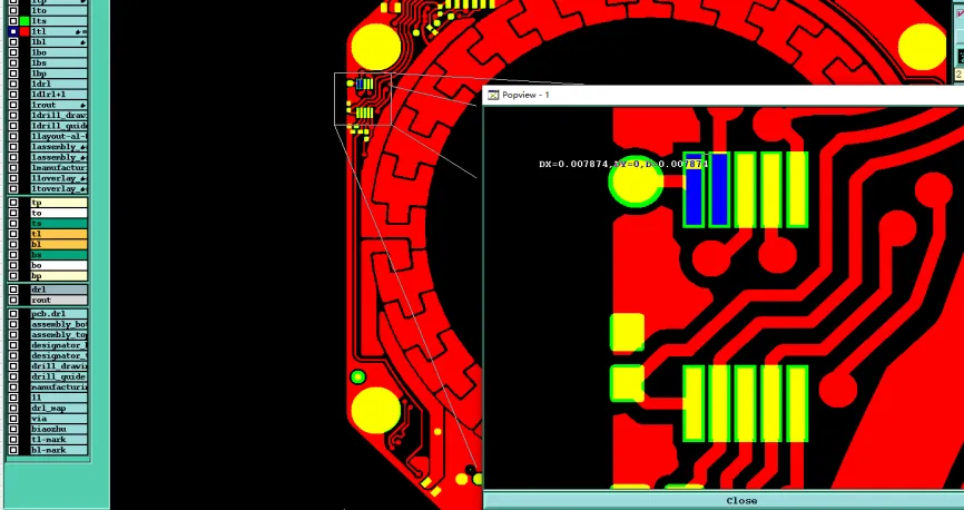
Our first review step involves verifying finished copper weight against actual trace geometry. We noticed a direct conflict: the provided data indicated 2oz outer copper, yet some internal notes or prior versions referenced heavier copper expectations. More critically, the minimum line spacing measured only 6.89mil in several areas.
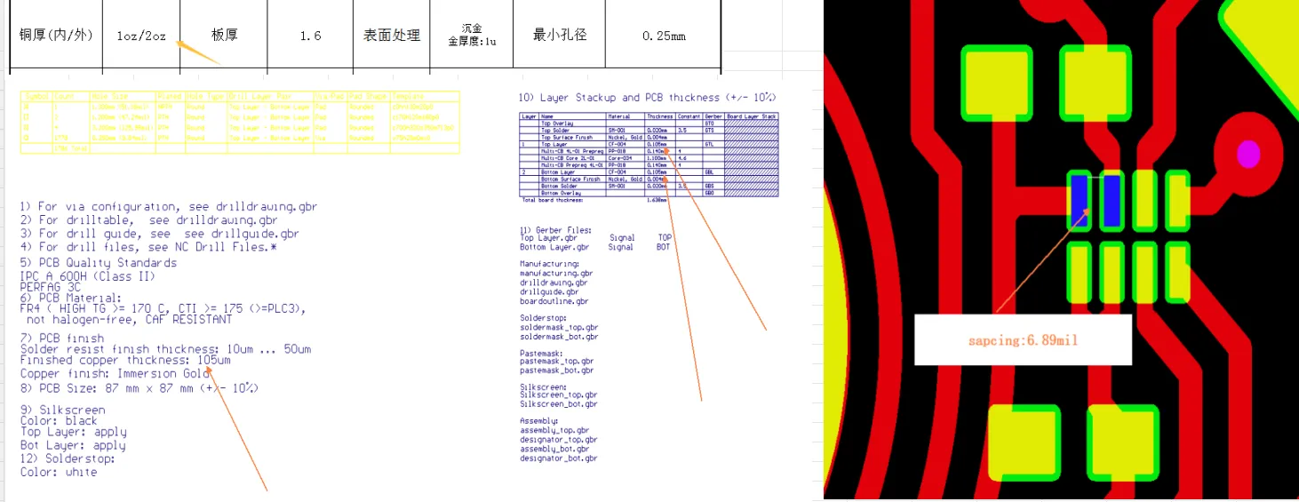
Figure 1: the minimum line spacing measured only 6.89mil in several areas
We confirmed with the team: "Our CAM engineer identified that 3oz copper capability requires at least 8mil spacing for reliable etching control. With only 6.89mil, proceeding at higher copper weight would risk severe undercutting and line width reduction beyond tolerance." If ignored, this could result in open circuits, excessive impedance variation, or complete trace breakage during etching — leading to high scrap rates and delivery delays.
Solder Mask & Silkscreen Issues
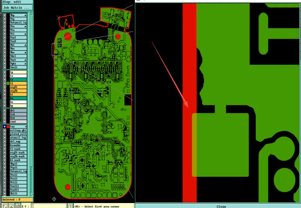
The most recurring EQs focused on BGA and IC pad regions where pad-to-pad spacing was only 7.87mil. For 2oz copper, standard solder mask bridge width becomes challenging due to the thicker copper profile and associated solder mask expansion/registration tolerances.

Figure 2: pad-to-pad spacing was only 7.87mil
We raised multiple confirmation points: the original design clearance was insufficient to guarantee a reliable solder mask dam (bridge) between pads. Our standard process for 2oz would result in mask slumping or incomplete coverage, risking solder bridging during assembly.
"After reviewing the BGA region in the Gerber files," our engineer noted, "we saw that 2oz copper combined with 7.87mil spacing left no room for a conventional mask bridge. We recommended switching to solder mask defined (SMD) pads — where the mask opening defines the pad size rather than the copper." This approach ensures a mask bridge exists while keeping the final exposed pad dimensions consistent. The customer needed to accept that some ink might overlap pad edges slightly, though finished BGA pad size remains unchanged.
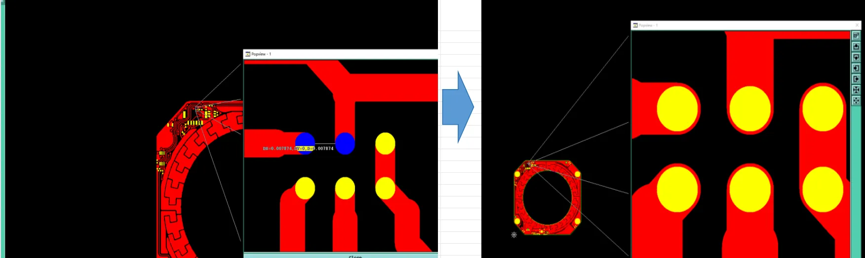
Figure 3: switching to solder mask defined (SMD) pads
Additional notes highlighted small IC pad widths, making pad shaving for bridge creation inadvisable as it would compromise solder joint reliability. If unaddressed, consequences could include solder shorts between pads, poor wetting, assembly yield loss, or intermittent connections in the field — especially problematic under thermal cycling given the TG170 specification.
Manufacturing Risks and DFM Insights
This case highlights two common customer design pitfalls: assuming uniform copper weight capability across all spacings and underestimating solder mask constraints on thicker copper. Many designers work from 1oz rules and then switch to 2oz for current-carrying capacity without adjusting clearances.
If the copper thickness conflict had been ignored, etching non-uniformity could cause trace width loss exceeding 20%, violating impedance requirements (if any) and increasing resistance. In worst cases, this leads to delamination under load or thermal stress failures, particularly with TG170 material that is expected to perform at elevated temperatures.
For the BGA solder mask issue, proceeding without SMD adjustment would likely produce insufficient mask dams. During reflow, solder could bridge adjacent pads, causing short circuits detectable only after assembly — resulting in costly field returns. According to typical IPC-6012 performance criteria, such defects would fail visual and electrical acceptance.
These issues often trigger multiple review cycles, extending lead times beyond the 11-day target and increasing engineering overhead. Our experience shows that early EQs like these prevent downstream assembly problems and protect overall yield.
How the Engineering Team Resolved the Issues
We compiled a clear EQ document with annotated screenshots (as referenced in the original review) and sent it to the customer for confirmation. For copper thickness, we clarified the feasible finished weight based on actual data geometry and recommended sticking to 2oz outer layers with verified spacing adjustments where possible.
"Our team suggested processing the BGA pads as solder mask defined," I noted internally during the review. "This maintains the required mask bridge without reducing copper pad area, aligning with common high-reliability practices for 2oz designs." The customer accepted this after we provided visual mockups showing final pad appearance.
Additional optimizations included confirming High TG material lot (FR-4 TG170), verifying ENIG thickness at 1U", and ensuring solder mask alignment data was updated. All changes were documented in the production traveler and CAM files. This collaborative workflow minimized risk while respecting the original design intent.
Final Manufacturing Outcome
After receiving customer confirmation on copper weight (2oz outer) and solder mask defined pad treatment for BGA regions, the engineering file was updated and released for production. The board passed internal DFM validation, with adjusted parameters ensuring etching uniformity and solder mask integrity. Production proceeded on schedule with 100% flying probe testing as requested.
Key Takeaways for PCB Designers
- Always verify minimum spacing requirements against your chosen finished copper weight. 2oz copper typically needs 8mil+ clearance for reliable etching in standard processes.
- For dense BGA or QFN areas on thicker copper, consider solder mask defined (SMD) pads early in layout to guarantee mask dams.
- Provide clear layer stackup and copper weight specifications in fabrication notes. Ambiguity triggers EQs and delays.
- Review Gerber files for actual minimum features before release — design software DRC may not fully reflect fabricator capabilities.
- High TG materials are excellent for thermal performance but still require careful copper and mask balancing to avoid warpage or delamination risks.
- Include tolerance expectations and reference drawings when possible. This helps CAM engineers align quickly.
- Communicate promptly on EQs — small clarifications prevent major production issues downstream.
FAQ
Q1: Why does 2oz copper require larger spacing than 1oz for solder mask bridges?
A1: Thicker copper increases the aspect ratio and sidewall profile, making solder mask application more prone to thinning or bridging failure in tight gaps. Standard processes need extra clearance (typically 7.5-8mil+) to ensure a reliable mask dam.
Q2: What is the advantage of solder mask defined pads in BGA regions?
A2: SMD pads allow the mask opening to control the exposed area, preserving a mask bridge between pads even when copper-to-copper spacing is marginal. This reduces solder bridging risk while maintaining consistent pad geometry for assembly.
Q3: Can tight spacing with heavy copper lead to etching problems?
A3: Yes. Insufficient spacing can cause etchant trapping, undercutting, and trace width reduction. In severe cases, this leads to opens, high resistance, or weakened mechanical strength — failing IPC-6012 criteria.
Q4: Why do factories raise EQs instead of making unilateral changes?
A4: Unilateral changes risk deviating from customer design intent. EQs ensure alignment on critical features like pad treatment or copper weight that affect electrical performance, assembly, and reliability.
Q5: How does High TG material interact with these copper issues?
A5: TG170 improves thermal stability but does not relax etching or plating rules. Heavy copper on high-TG boards still demands adequate spacing to avoid stress concentrations that could cause warpage or delamination during thermal excursions.
Q6: What should designers do before submitting 2oz designs?
A6: Run a detailed DFM check against your fabricator's 2oz design guidelines. Pay special attention to BGA/IC clearances and include copper weight clearly in the fabrication drawing.