PCB Specifications
| Parameter | Value | Parameter | Value |
|---|---|---|---|
| PCB Type | FR4 PCB | Quantity | 200 pcs |
| Layers | 2 Layers | Board Type | Single PCB |
| Dimensions | 87 x 87 mm | Copper Weight | 2oz |
| Thickness | 1.6 mm | Min Track / Spacing | 6/6mil↑ |
| Surface Finish | ENIG (Immersion Gold) | Min Hole Size | 0.25mm |
| Solder Mask | White | Silkscreen | Black |
| Stack-up | Custom | Impedance Control | No |
Manufacturing Timeline
Logistics Information
Key Manufacturing Processes
Manufacturing Summary
This 2-layer FR-4 board measured 87 × 87 mm with 1 oz inner and 2 oz outer copper and a 1.6 mm finished thickness using KB-6167F TG170 material. Produced in a high-volume run of 200 pieces as single boards, the design featured standard 6 mil line/space, ENIG surface finish, and a high hole density of 236000 per square meter. No impedance control or blind vias were required, with mechanical forming and 100% flying probe testing. UL marking was requested without the provided logo file.
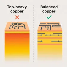
DFM review identified copper thickness conflicts. The specified 3 oz outer copper could not be achieved due to 6.89 mil minimum spacing falling below the 8 mil threshold for reliable 3 oz processing. For 2 oz copper, BGA and IC pad areas with 7.87 mil spacing prevented solder mask bridges. These features were processed as solder mask defined pads to guarantee bridge integrity, accepting partial ink coverage around pads while keeping final pad dimensions unchanged. Multiple confirmations resolved the approach for both BGA and trace areas.
Production completed within 11 days with all electrical and dimensional parameters met. The higher outer copper weight and dense via pattern were consistently achieved, delivering boards with good thermal and mechanical properties for this volume order.
Explore More PCB Manufacturing Resources
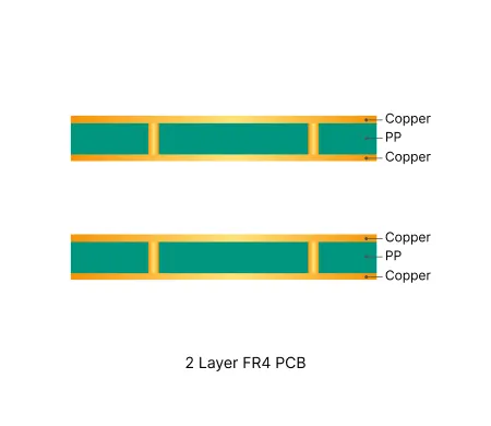
2 Layer FR4 PCB Manufacturing Insights
2 layer FR4 PCBs deliver cost-effective solutions for most electronic designs. Their simple structure enables consistent quality and efficient production cycles.
Why 1 Layer and 2 Layer FR4 PCB Trigger Frequent Engineering Queries in Production
Real Engineering Queries (EQ) and DFM issues for 2 Layer FR4 PCB (double-sided boards) from actual production reviews. Learn how to avoid common problems with via treatment, silkscreen on pads, solder mask openings, hole attributes, board edge clearance, and other frequent design pitfalls.
Real Production Records
| Order ID | PCB Type | Layers | Dimensions | Solder Mask | Surface Finish | Quantity | Action |
|---|---|---|---|---|---|---|---|
| FR4-20260528-028 | FR4 PCB | 2 | 185 x 245 | Green | HASL Lead Free | 5 | View detail |
| FR4-20260526-001 | FR4 PCB | 2 | 100 x 100 | Green | HASL Lead Free | 10 | View detail |
| FR4-20260525-001 | FR4 PCB | 2 | 50 x 45 | Matte Green | HASL Lead Free | 20 | View detail |


