In PCB manufacturing, even seemingly straightforward 6-layer boards can present multiple manufacturability hurdles during engineering review. This case study examines a recent 6-layer FR-4 order (#FR4-20260430-043) where the combination of tight BGA via specifications, inconsistent solder mask requirements, silkscreen placement issues, and detailed post-fabrication labeling created several engineering questions (EQs) during CAM preparation.
Our CAM team identified risks that could lead to short circuits, poor assembly yield, and cosmetic defects if left unaddressed. This article details the actual engineering review process, the specific issues found, the risks involved, and how we resolved them through clear communication and data optimization.
Order Overview
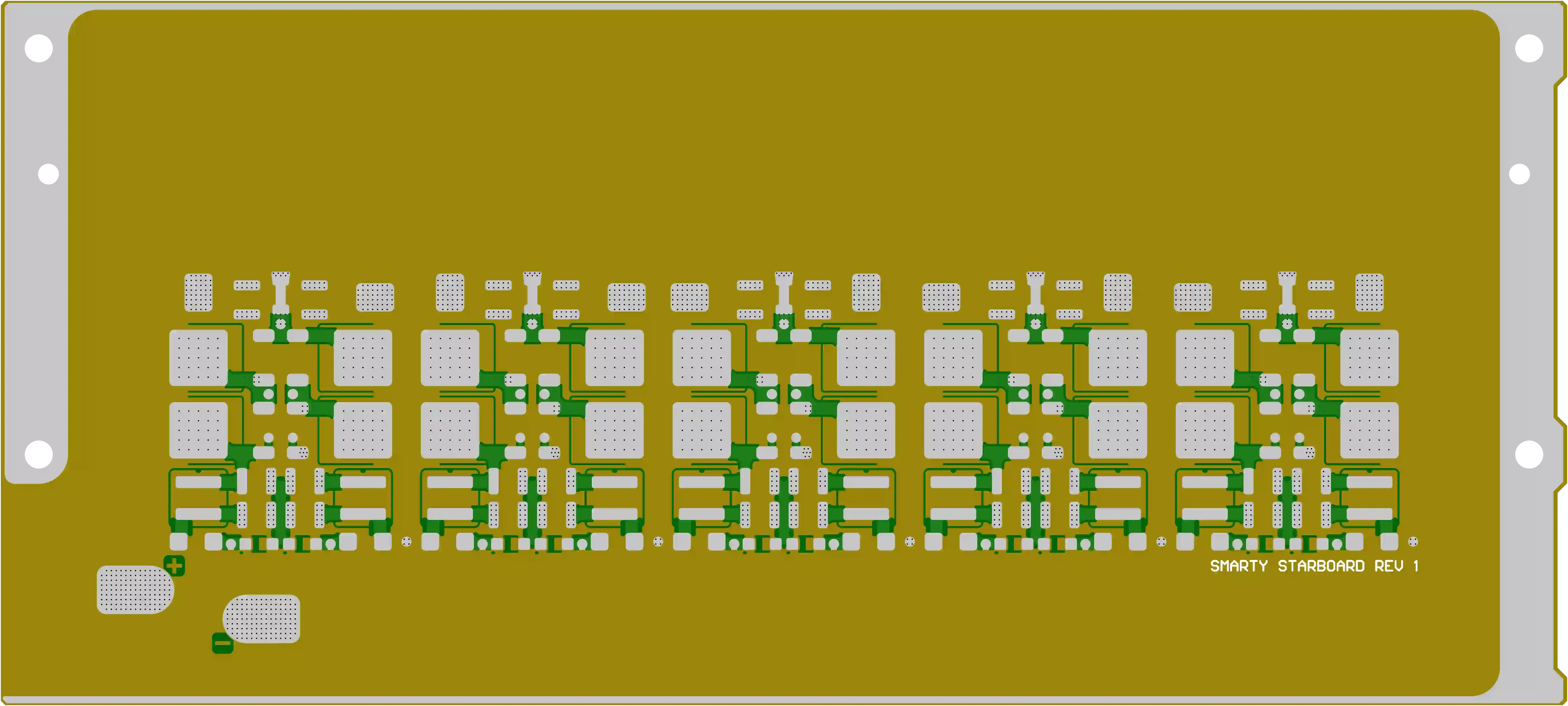
This was a standard 6-layer rigid PCB fabricated on FR-4 material with TG150 rating. Board dimensions were 171.2 × 305 mm, with a finished thickness of 1.6 mm. Copper weight was specified as 1 oz inner and outer layers. The design called for a minimum hole size of 0.1 mm, 100% flying probe testing, and lead-free HASL surface finish with green solder mask and white silkscreen.
Panelization was single-board (1x1) with V-scoring. Quantity was only 5 pieces with an 8-day delivery window. The customer explicitly noted "vias per Gerber" and accepted our suggested lamination approach while requesting specific documentation review for labeling requirements. Although the layer count and material were conventional, the combination of fine features, BGA areas with mixed solder mask openings, and post-process marking instructions triggered detailed DFM scrutiny.
Main Engineering Questions Found During CAM Review
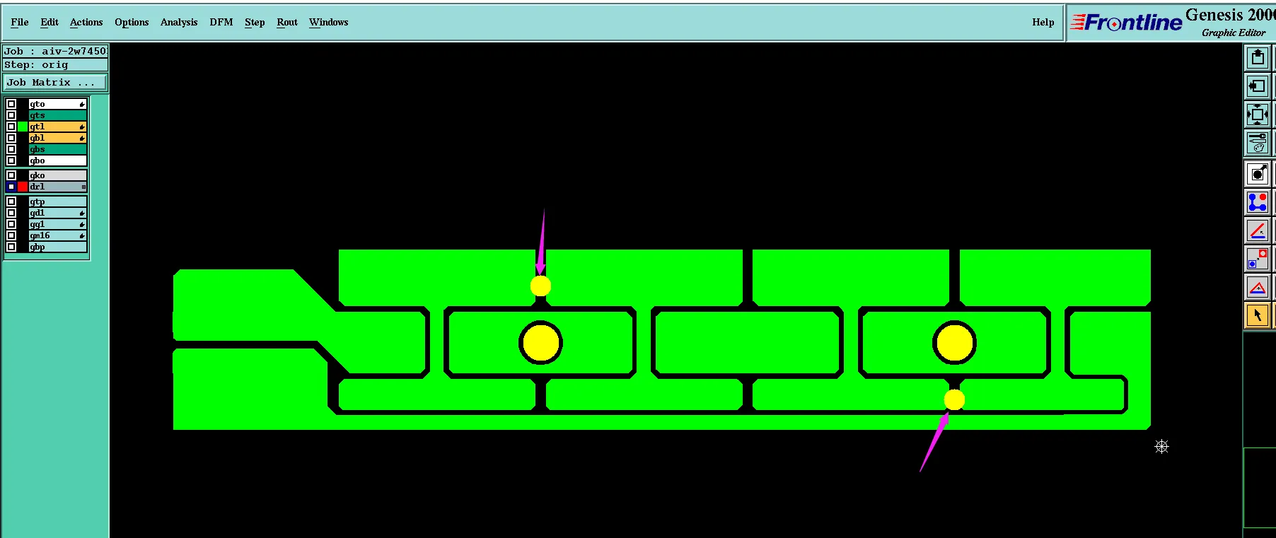
1. BGA Solder Mask Windowing Inconsistency and Via Treatment Risk
Our engineer noticed that in the provided Gerber data, certain BGA regions had single-sided solder mask openings while others used double-sided openings. The customer's fabrication note clearly stated "vias per Gerber" meaning vias in these areas should follow the original design intent without additional tenting or plugging.
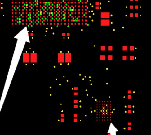
Figure 1: BGA regions had single-sided solder mask openings while others used double-sided openings.
We identified a potential short circuit risk where vias placed under or near BGA pads could remain exposed or have inconsistent coverage after HASL processing. If the mixed windowing was not clarified, exposed copper or insufficient solder mask dam between vias and pads could lead to solder bridging during SMT assembly.
Our CAM team flagged this immediately. We suggested confirming the exact intent for each BGA zone and recommended selective via tenting where manufacturability allowed, while preserving the customer's "per Gerber" requirement in critical signal areas. Ignoring this could have resulted in assembly failures, rework, or complete board scrap due to electrical shorts.
2. Silkscreen Characters Overlapping Pads
Another clear issue was silkscreen legends placed directly on component pads in multiple locations. This is a common design oversight that becomes critical during production. We noticed the characters would interfere with solder paste application and component placement if printed as-is.
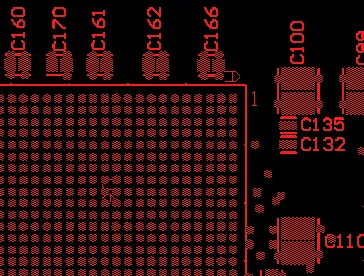
Figure 2: Silkscreen legends placed directly on component pads
Our standard practice in such cases is to either move the legend or request customer approval for removal in pad areas. In this order, we raised an EQ with annotated screenshots showing the overlapping regions. If left unchanged, this could cause poor solderability, tombstoning, or unreliable electrical contact after assembly.
3. Custom Post-Fabrication Labeling with Stickers and Serial Numbers
The customer provided specific instructions for applying non-adhesive labels (stickers) at designated positions to mark component version letters and manufacturing serial numbers. They requested us to generate sequential numbering such as D260323000, D260323001, etc.
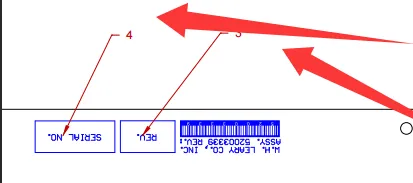
Figure 3: Component version letters and manufacturing serial numbers with non-adhesive labels techniques
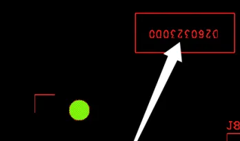
Figure 4: Sequential numbering silkscreen
Our engineering team reviewed the placement locations and proposed the exact text format. We asked for confirmation on whether our generated numbering and positioning were acceptable. While not a core manufacturing risk, unclear labeling can cause traceability issues downstream in the supply chain. We also needed to ensure the sticker application process would not damage the board surface or affect impedance-critical areas.
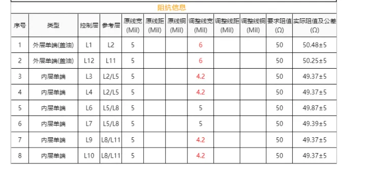
4. Lamination Stackup Confirmation After Internal Adjustment
Although the customer accepted our suggested close-to-original lamination approach, we provided a revised stackup diagram for final approval. For a 1.6 mm 6-layer board with 1 oz copper, maintaining symmetric copper distribution and proper prepreg thickness is essential to control warpage and ensure reliable via plating.
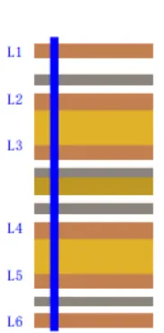
Figure 5: Revised stackup diagram
We noticed minor adjustments were necessary to meet both impedance targets (implied by the design) and our process capabilities. After reviewing the stackup, we confirmed the revised structure with the customer before proceeding to inner layer imaging.
Manufacturing Risks and DFM Insights
This case highlights several recurring DFM challenges in multi-layer boards with dense BGA regions. The mixed solder mask opening approach combined with "vias per Gerber" increases the chance of exposed copper after surface finish, potentially leading to edge shorts or corrosion over time. If ignored, hole breakout or unreliable plating in 0.1 mm vias could cause open circuits or high resistance paths.
Silkscreen on pads is a frequent trigger for EQs. According to typical IPC-A-600 acceptability criteria, legend ink on pads is considered a defect that can compromise solder joint integrity. In high-volume production, this would lead to significant yield loss and assembly line stops.
Custom labeling, while secondary, adds complexity to the final QC and packaging stages. Poorly defined serial number formats can result in mislabeled boards and traceability failures during customer incoming inspection.
How the Engineering Team Resolved the Issues
Our CAM engineer suggested adjusting the solder mask data for BGA areas after receiving customer confirmation on the mixed windowing intent. We generated modified Gerber files that preserved critical vias while ensuring adequate solder mask dams where possible.
For the silkscreen overlap, we proposed removal of conflicting legends and provided before/after comparisons. The customer approved the changes quickly, avoiding potential assembly defects.
Regarding labeling, we confirmed the serial number sequence and sticker positions. The revised stackup was also approved without major iteration. All modifications were documented and version-controlled before releasing the job to production.
Final Manufacturing Outcome
After addressing all EQ points, the engineering data package was finalized and approved by the customer. The order was released for inner layer processing with optimized panelization and process parameters. Production proceeded on schedule within the 8-day window.
Key Takeaways for PCB Designers
- Always maintain consistent solder mask definitions across similar component areas, especially BGAs. Mixed single/double-sided openings require explicit documentation.
- Avoid placing silkscreen legends on component pads. Provide clear keep-out zones in your design rules.
- When specifying "vias per Gerber" ensure via-to-pad clearances meet both your electrical needs and the fabricator's minimum annular ring requirements (typically per IPC-6012).
- Provide detailed, annotated drawings for any post-fabrication marking or labeling requirements to reduce back-and-forth communication.
- Include a complete stackup diagram with layer thicknesses and materials when submitting files, even if accepting factory suggestions.
- Define serial number formats and positioning early to allow CAM engineers to incorporate them without affecting copper or mask layers.
- Review your Gerber files for copper islands or isolated features near V-scores that could cause etching or depanelization issues.
FAQ
Q1: Why do PCB factories raise concerns about mixed BGA solder mask openings?
A1: Mixed openings can lead to inconsistent solder mask coverage around vias. This increases the risk of solder bridging or exposed copper after HASL, potentially causing short circuits during assembly.
Q2: What happens if silkscreen is printed on component pads?
A2: Legend ink interferes with solder paste deposition and component seating, leading to weak joints, tombstoning, or open circuits. Most fabricators will request removal or relocation.
Q3: Why is stackup confirmation important even when the customer accepts factory suggestions?
A3: Slight adjustments to prepreg and core thicknesses can affect impedance, warpage, and via reliability. Formal confirmation ensures the final board matches both electrical and mechanical requirements.
Q4: How should designers specify custom serial number labeling?
A4: Provide a clear drawing with exact positions, font size, content format, and any special requirements (e.g., sticker type). This allows the factory to integrate it cleanly without affecting functional layers.
Q5: What is the risk of not clarifying "vias per Gerber" instructions?
A5: Vias may receive unintended tenting or plugging, altering signal integrity or causing plating defects. In worst cases, it leads to functional failures after assembly.
Q6: Can small-order prototypes (5 pcs) still benefit from full CAM review?
A6: Yes. Early detection of issues like those in this case prevents costly scrap and schedule delays, especially when tight tolerances and custom requirements are involved.