6 Layer FR4 PCB Production Record #FR4-20260430-043
| Parameter | Value | Parameter | Value |
|---|---|---|---|
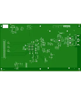
| PCB Type | FR4 PCB | Quantity | 5 pcs |
| Layers | 6 Layers | Board Type | Panel PCB |
| Dimensions | 171.2 x 305 mm | Copper Weight | 1oz |
| Thickness | 1.6 mm | Min Track / Spacing | 5/5mil |
| Surface Finish | HASL Lead Free | Min Hole Size | 0.1mm |
| Solder Mask | Green | Silkscreen | White |
| Stack-up | Default | Impedance Control | No |
This 6-layer FR-4 PCB measured 171.2 × 305 mm with 1.6 mm finished thickness and 1 oz copper on both inner and outer layers. We produced five pieces using standard FR-4 material (TG150) and applied lead-free HASL surface finish with green solder mask and white silkscreen. Minimum hole size reached 0.1 mm and line width/space was controlled at 5 mil, placing the design in the tighter geometry range for a 6-layer board. V-cut panelization was used with 1-up single panel format and mechanical forming for the final outline.
During CAM review, several DFM issues required attention. The original Gerber files showed inconsistent BGA solder mask openings—some single-sided and others double-sided—which created short-circuit risks during assembly. Silkscreen elements also overlapped pads in multiple locations. Additionally, the customer requested custom non-conductive sticker labeling at specific positions for component version letters and sequential serial numbers (D260323000 series). We adjusted the lamination stack-up to meet the specified press requirements while maintaining layer registration. All modifications were reviewed and confirmed with the customer before proceeding to production.
These BGA solder mask and silkscreen adjustments ensured reliable solderability and assembly compatibility. The boards completed 100% flying probe testing with no impedance requirements. Production ran smoothly within the 8-day delivery window, with final electrical test reports and quality certificates provided. The order was shipped successfully with full traceability for the custom markings.
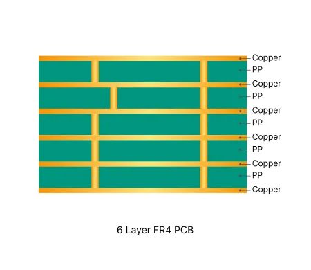
Six layer FR4 boards provide optimized routing density and power distribution. They require precise lamination and plating process control to maintain yield and reliability.

In-depth guide to the most frequent Engineering Queries (EQ) and DFM issues in Multilayer FR4 PCB (4/6/8+ layers) production. Real factory insights on stack-up confirmation, impedance control, copper balance, inner layer design, via treatment, registration, and practical prevention strategies.
| Order ID | PCB Type | Layers | Dimensions | Solder Mask | Surface Finish | Quantity | Action |
|---|---|---|---|---|---|---|---|
| FR4-20260628-010 | FR4 PCB | 2 | 60 x 120 | Green | HASL Lead Free | 5 | View detail |
| FR4-20260619-010 | FR4 PCB | 2 | 121 x 121 | Green | HASL Lead Free | 50 | View detail |
| FR4-20260618-018 | FR4 PCB | 2 | 54.74 x 106.93 | Green | HASL Lead Free | 5 | View detail |


