










A simple 1-layer FR4 PCB order with OSP surface finish and mechanical forming requirements entered CAM review. The order specified single piece delivery with V-CUT, yet production data showed panelized layout with a 1mm process edge that prevented standard V-CUT processing. This core misalignment between order intent and actual files triggered detailed engineering investigation to determine manufacturable configuration.
With 11-day delivery and full electrical testing planned for 10 pieces, quick resolution was essential. Additional observations on hole attributes, process edges, and Gerber layer discrepancies further highlighted interpretation challenges for this seemingly straightforward single-layer board.
Understanding the Original Design Intent
The customer aimed for a basic single-layer board ( #FR4-20260507-117 ) measuring approximately 20x96mm using TG150 FR4 material at 1.6mm thickness. Key features included 0.8mm holes, OSP finish, black solder mask and silkscreen, with customer self-panelization noted. The intent was cost-effective production of functional single-sided circuitry suitable for electronic applications requiring standard mechanical forming.
Fabrication notes emphasized no process edge and single piece output with V-CUT. However, the submitted Gerber data presented a panelized layout with maximum outline dimensions, creating immediate questions about how to achieve the ordered delivery format while respecting the physical data provided.
Engineering Findings During Initial CAM Review
Our CAM engineer observed that the production data was panelized despite the system order for single pieces. The maximum outer frame dimensions made standard V-scoring impossible without adjustment. Further examination revealed a 1mm process edge in the files that conflicted with the "no process edge" requirement.
Hole attributes for certain plated and non-plated holes needed confirmation, particularly where copper connections appeared on one side. Gerber layers showed bottom PADs despite single-layer designation, adding to the interpretation complexity.
| Observation | Data Source | Identified Issue |
|---|---|---|
| Panelized layout vs single piece order | Gerber vs Order specs | V-CUT incompatibility |
| 1mm process edge present | Fabrication data | No process edge requirement |
Primary Conflict: Panelization and Process Edge Interpretation
The dominant conflict was a Manufacturing Interpretation Conflict regarding panelization method and process edge handling for single piece delivery. The order called for individual boards with V-CUT, but the actual Gerber data used a panelized format with a 1mm process edge that could not be V-CUT within the maximum outline dimensions. This prevented straightforward production matching the delivery specification.
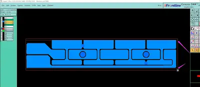
Figure 1: maximum outer frame dimensions made standard V-CUT impossible
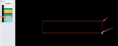
Figure 2: the 1mm edge rail in your file is not able to be V-cut
During verification, the design files and order requirements could not be aligned without clarification. Production could not proceed because ignoring the panelization would result in incorrect delivery format, while forcing V-CUT on the provided data risked incomplete separation or dimensional inaccuracies. Our team evaluated both routing and alternative depanelization options based on the physical layout evidence.
"Further review revealed that the manufacturing intent for single piece output could not be reliably achieved with the submitted panel data," noted during analysis. Per IPC-A-600 considerations for board outline processing, such mismatches often lead to mechanical defects if not resolved prior to fabrication.
If left unaddressed, this could cause boards to be delivered as connected panels instead of individuals, complicating customer assembly, or result in rough edges from forced processing. The conflict centered on translating customer delivery expectations into compatible production steps.
Supporting Hole and Layer Observations
Additional findings included plated holes with 1:1 pad connections and copper on one side requiring attribute confirmation to avoid unintended shorts or open circuits. Two non-copper holes lacked proper clearance treatment. The Gerber files contained bottom layer PADs despite the single-layer description, suggesting possible data export anomaly. Production numbering addition was straightforward but needed positioning confirmation.
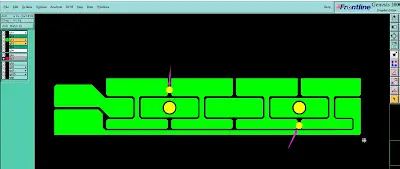
Figure 3: the hole indicated by the arrow is aligned 1:1 with the pads on both sides
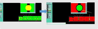
Figure 4: shave the copper as our factory standard
These elements supported the main panelization investigation by underscoring broader data consistency needs for this single-layer job.
| Issue | Evidence | Risk Level |
|---|---|---|
| Hole copper connections | Gerber layers | Low - Attribute confirmation |
| Bottom PADs in single layer file | Layer data | Low - Data cleanup |
Engineering Clarification and Final Resolution
The 1-Layer FR4 PCB EQ detailed the panelization mismatch with annotated images of the maximum outline and process edge. We proposed options including individual routing from the panel data or customer confirmation on accepting panel delivery with manual separation. Hole attributes, clearance treatments, and numbering placement were also addressed with specific recommendations.
Customer confirmation aligned on processing the panel data into single pieces via routing where V-CUT was not feasible, accepted minor adjustments for hole treatments, and verified Gerber layer intent. Revised production files reflected these decisions, enabling clean mechanical forming and delivery as individual boards.
Key Design Lessons for PCB Designers
- Match panelization approach in Gerber data to the ordered delivery format (single piece vs panel).
- Clearly specify process edge requirements and ensure data files reflect them accurately.
- Verify V-CUT feasibility against actual board outline dimensions before submission.
- Provide consistent layer information for single-layer designs to avoid export artifacts.
- Define hole attributes including copper clearance for non-plated features explicitly.
- Confirm production numbering content and location to prevent placement conflicts.
- Cross-check all files for internal contradictions between order notes and manufacturing data.
- Consider routing as alternative when V-CUT is incompatible with panel layout.
FAQ
Q1: Why does panelized data conflict with single piece orders?
A1: The physical layout in Gerber files may not support V-CUT within specified dimensions, requiring clarification on depanelization method to match delivery expectations.
Q2: What issues arise from process edges in "no edge" designs?
A2: Extra edges can interfere with V-CUT or routing, leading to dimensional inaccuracies or additional processing steps if not aligned with order requirements.
Q3: How should single-layer Gerbers be validated?
A3: Ensure only top layer features are present and bottom PADs are absent or intentional. Inconsistencies often indicate export errors needing correction.
Q4: When is routing preferred over V-CUT for depanelization?
A4: When panel dimensions or process edges prevent clean V-CUT, routing individual boards from the panel ensures accurate single piece delivery.
Q5: Why confirm hole attributes during CAM review?
A5: Connections between pads and copper on specific sides can affect functionality. Clarification prevents unintended shorts or manufacturing defects.






