These situations are common in PCB design: BGA escape routing looks clean, yet a high-speed link drops packets in test; a multilayer board comes back warped; solder yield falls sharply.
The cause is often not the IC and not the fabricator. It is via fanout. The following practical rules cover via function, size, spacing, IC and capacitor fanout, board-edge grounding, BGA escape, copper pour, differential vias, and shared vias.
1. Via Function and Basic Rules
A via is the path a signal uses to change layer.
- It must connect across layers. Do not leave a via attached to only one layer and create a stub, except for thermal vias.
- Prefer a larger hole diameter when possible. That raises fabrication yield and lowers cost.
2. Via Types and How Many to Use
- Do not use more than three via types in one design.
- Common sizes: 8/16, 10/22, 12/24
- HDI: 4/10 and 4/8 laser vias
- Thicker boards need larger holes. On a 2-layer board, 12/24 is recommended.
Too many via types increase process difficulty and cost.
3. Current Capacity: Add Via Margin
Vias carry current as well as signals.
Place vias at about twice the calculated count so the electrical design has margin.
4. Via Pitch Affects Power Integrity
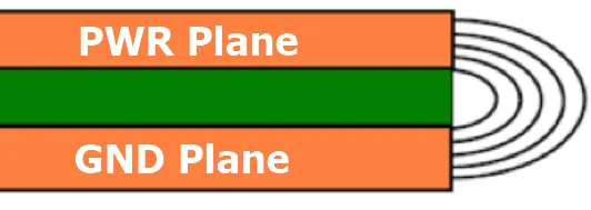
If vias are too close, they can cut the ground or power plane and raise EMI.
Keep center-to-center spacing ≥ 1 mm (39.37 mil) so traces can still pass and plane integrity is kept.
5. IC and Capacitor Fanout
- IC fanout: escape toward the outside first and keep left and right vias on the same horizontal line so inner-layer routing is easier.
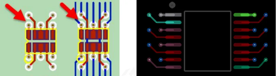
- Capacitor fanout: shorten the loop. Do not place the via in the center of the pad, which can cause poor soldering.
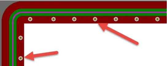
6. Board-Edge Shield GND Vias
Place a ring of GND vias along the board outline at 50–200 mil spacing to form a shield.
7. BGA Fanout
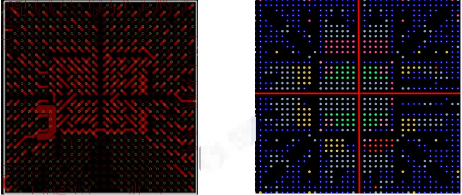
- Place vias at the diagonal center of the pads. Keep the center cross channels free of vias.
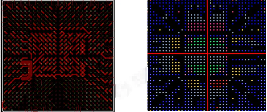
- The first two rows of vias can be shifted outward and aligned with the inner vias so inner-layer escape is easier.
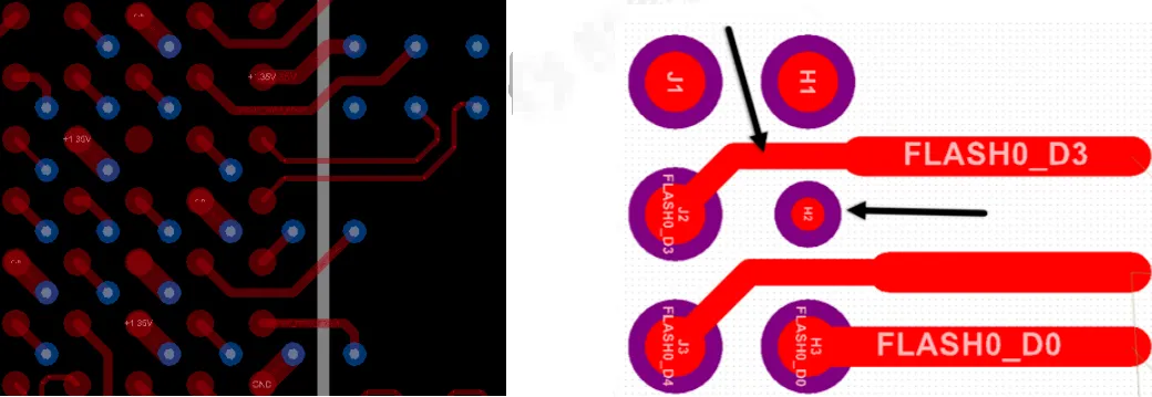
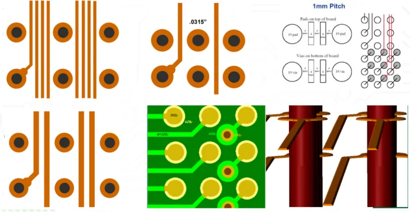
- If BGA pitch is ≥ 1 mm, two traces can pass between vias. If pitch is < 1 mm, only one trace can pass. A 0.4 mm pitch needs HDI.
8. Copper Pour and Isolated Copper
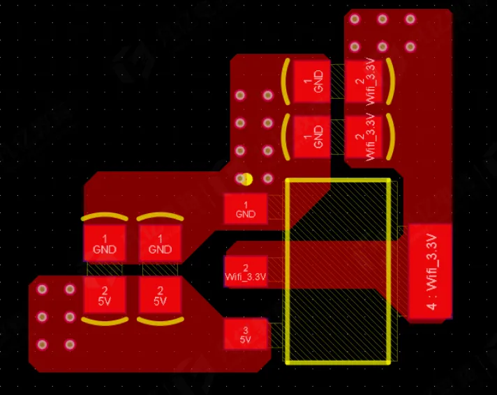
- For parts larger than 0805, use a cross connection to the pour to reduce soldering defects.
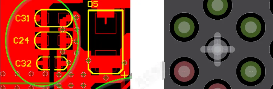
- Avoid large areas with no copper, which can warp the laminate.
- After routing, clean the pour: remove sharp corners and isolated copper.
9. Differential-Signal Vias
- When a pair changes layer, add nearby GND vias to shorten the return path.
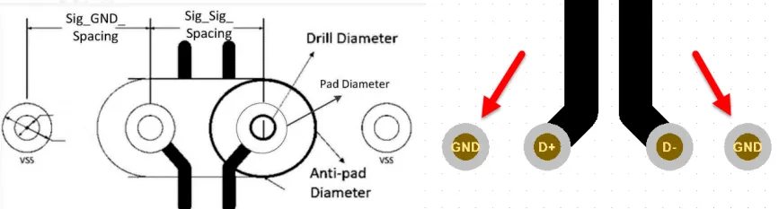
- Keep clearance between the differential vias. Do not route another signal between them.
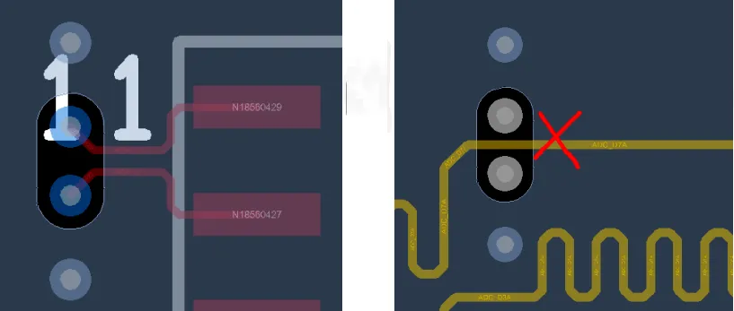
- Keep the pair symmetric and coupled, and minimize the uncoupled length.
10. Shared Vias and High-Speed Connectors
- BGA power or ground pins may share a via, but only for two pins. Do not share one via among more pins.
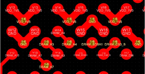
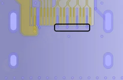
- On a high-speed connector, place at least one GND via on each ground pad, as close to the pad as possible.
Summary
Via fanout looks like a small drilling choice. It affects signal integrity, electrical performance, fabrication yield, and cost. These rules make the PCB more stable to build and more consistent in test.