Hardware designers are familiar with the LDO, or low-dropout regulator. It is a small part that supplies stable voltage to electronic equipment. Many designs fail at the PCB, not in part selection. Poor placement or routing can make the output voltage unstable, weaken immunity, and affect the whole product.
The points below cover LDO PCB design from the basic function through placement and routing.
What an LDO Is
LDO stands for low-dropout regulator. Its role is to step a higher voltage down to a lower voltage that ICs and circuits can use. In the description used here, it consists of a DC voltage regulator and a current amplifier. A controlled dropout between input and output keeps the output voltage from drifting.
Four characteristics explain why LDOs are widely used for local supplies:
- Low dropout: the dropout ranges from a few hundred millivolts to several volts, so a higher rail can be stepped down with a small headroom.
- Stable output: output voltage is less affected by input variation, with useful noise and interference rejection.
- Low power: linear regulation does not switch continuously, so consumption stays low.
- Fast response: the output can be adjusted quickly when the load changes, so the supply is not interrupted.
LDOs appear in phones, wearables, communications equipment, and embedded systems as a local regulator.
LDO PCB Placement: Two Points Matter Most
Placement is the base of the LDO layout. If placement is wrong, later routing will not recover the result. The governing rule is to keep the power loop as small as possible. Two practices implement that rule.
1. Use an In-Line or L-Shaped Placement
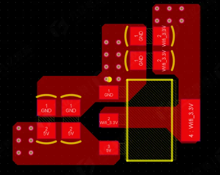
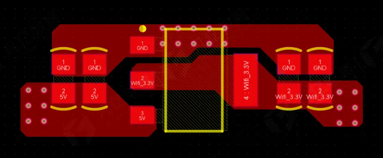
Follow the input-to-output flow and prefer an in-line (straight) or L-shaped placement. Both shorten the power loop, reduce interference and voltage drop, and avoid an unstable supply caused by a long loop.
2. Place Filter Capacitors Large Then Small
On both the input and the output, place the large capacitor first and the small capacitor next. That order helps remove ripple and keeps the input and output voltages steadier. Do not reverse the order.
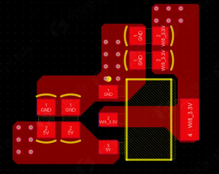
LDO PCB Routing: Four Rules
If placement is the frame, routing is the current path. Power and ground routing determine how well the LDO works. The four points below should not be skipped.
1. Size Power Traces and Vias for Current
Power-trace width and via count must match the actual current. Meet the current-carrying requirement so thin traces or too few vias do not cause heating and excessive voltage drop.
2. Place Input and Output Vias in the Correct Order
Place the input power via before the first filter capacitor. Place the output power via after the last filter capacitor. That via order keeps the capacitors in the path and lets the filtered supply continue cleanly.
3. Keep GND Wide and Put GND Vias Next to the IC Pins
Make the ground current path as wide as practical to lower ground resistance. Place GND vias together, close to the IC GND pins, so the ground loop stays short and the ground connection is more stable.
4. Connect Input Ground to Output Ground
Do not leave input ground and output ground disconnected. Join them reliably so the circuit has a continuous return path. A broken return produces noise and can disturb the output voltage.
Summary
LDO PCB design has many details, but the logic is short: shorten the loop, carry the current, keep ground stable, and filter in the correct order. An in-line or L-shaped placement with capacitors in large-then-small order, plus routing that meets current, via position, wide GND, and a continuous ground return, is what lets the LDO deliver a stable local supply and avoids common power-layout failures.