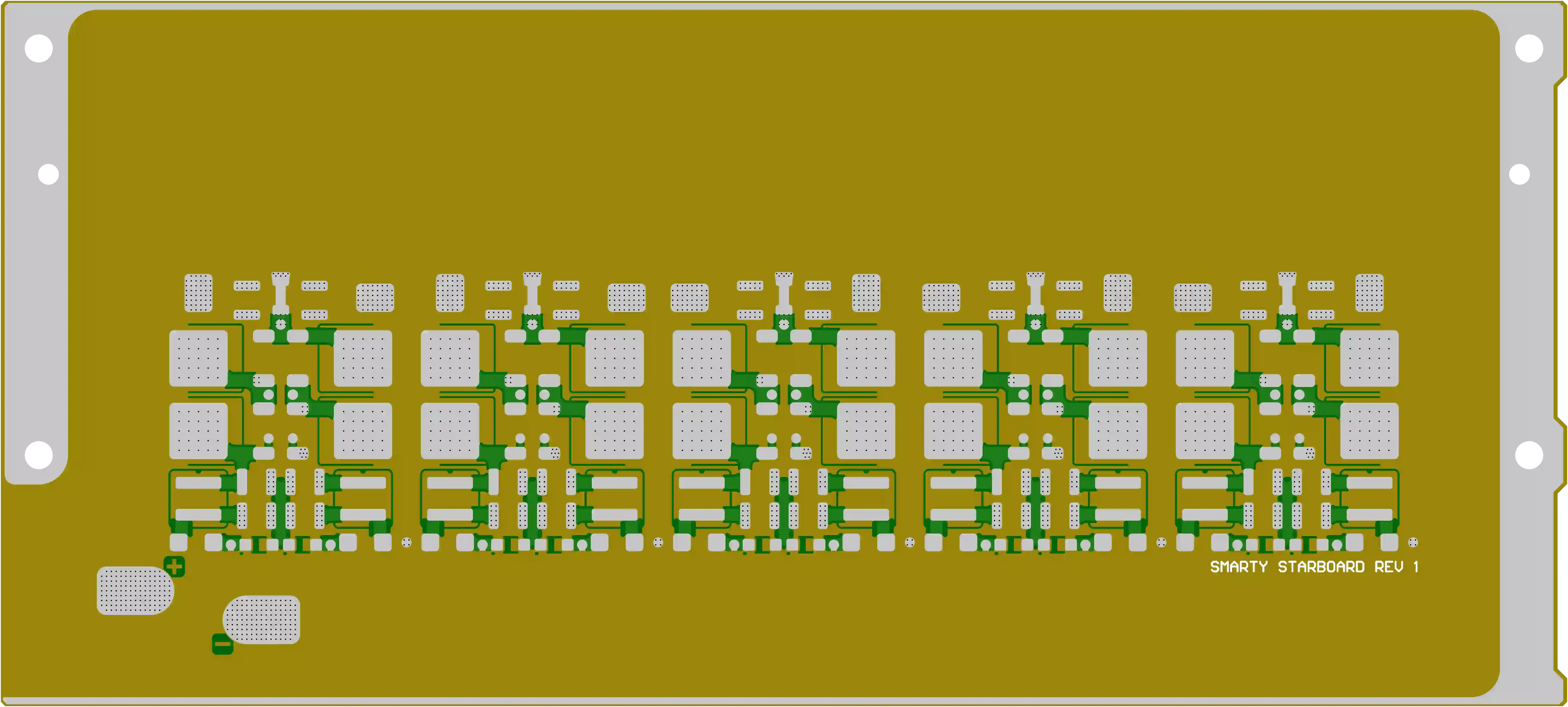
In March 2026, we reviewed an 8-layer PCB order sized 281 × 100 mm with 1.0 mm finished thickness and blind vias. Although standard FR-4 material and no impedance control were specified, the combination of dense SMD pad layout, NSMD BGA pads, mixed via solder mask treatments, and customer panelization created multiple critical DFM issues during CAM engineering review.
Boards with blind vias and tight SMD spacing frequently require detailed clarification. Our CAM team identified several manufacturability gaps that could lead to solder mask defects, assembly problems, or panel breakage. This real-world case shows why thorough engineering review remains essential even for conventional multi-layer designs.
Order Overview
This was an 8-layer FR-4 TG150 PCB ( #FR4-20260504-094 ) with 1 oz copper on inner and outer layers, 1.0 mm thickness, and ENIG surface finish. Minimum hole size was 0.3 mm with blind vias implemented. The design used customer self-panelization in 1×5 format with routing separation. Order quantity was 50 pcs (10 sets). 100% flying probe testing was required. No impedance control was specified, but precise solder mask and mechanical features demanded careful attention.
Special considerations included panelization details, stamp hole positioning, and BGA pad structure, making this a typical medium-volume job where DFM alignment between design intent and factory capability was crucial.
Main Engineering Questions Found During CAM Review
1. Solder Mask Bridge on Dense SMD Pads
Our CAM engineer identified multiple SMD pads with only 2 mil spacing. Our standard production capability requires a minimum 5.9 mil solder mask bridge to ensure reliable ink coverage and prevent bridging during assembly.
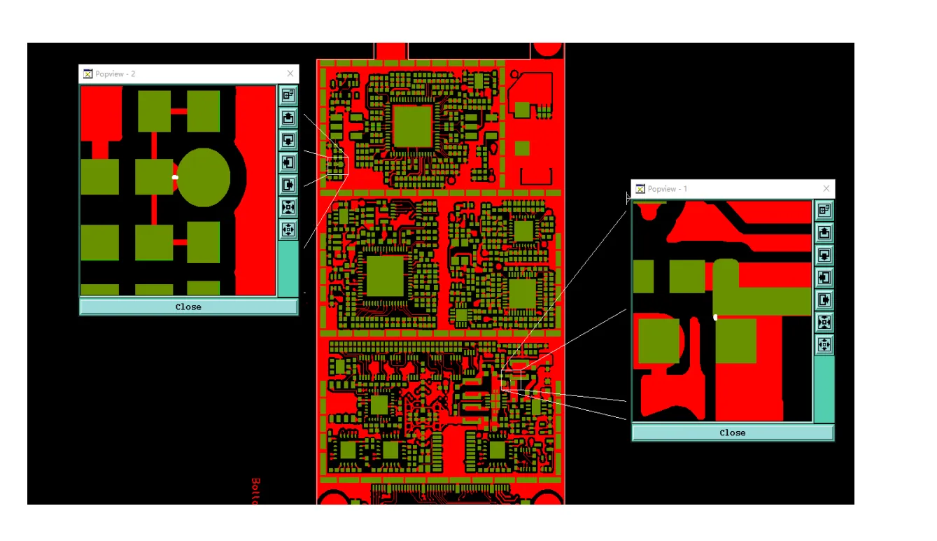
Figure 1: multiple SMD pads with only 2 mil spacing
We proposed adjustments and asked for confirmation. For one test point area (Popview), the customer suggested partial mask coverage or removal. This kind of tight spacing is common in dense designs but often conflicts with actual manufacturing tolerances.
If ignored, solder mask bridges would fail, causing solder shorts between pads during SMT, poor yield, and potential field failures. We have seen similar cases result in complete batch scrap after assembly.
2. NSMD BGA Pads and Via Windowing Risks
The Gerber data used Non-Solder Mask Defined (NSMD) pads for BGA areas. Our engineer raised concern about potential pad cratering (pit cracking) and reduced adhesion during thermal cycling. We also found inconsistent via solder mask treatment — some vias with double-side open window, others single-side covered, creating risk of exposed copper and tin whisker issues.
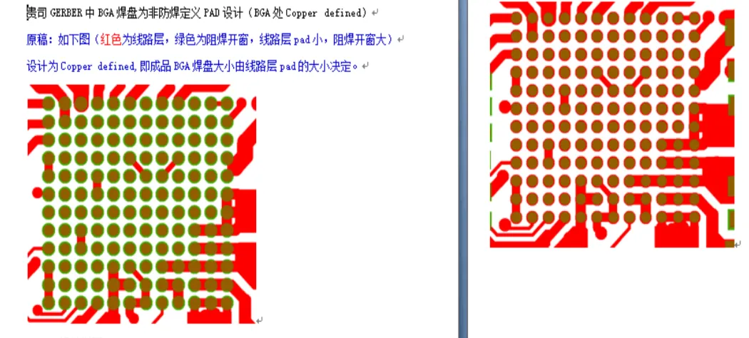
Figure 2: Gerber data used Non-Solder Mask Defined (NSMD) pads for BGA areas
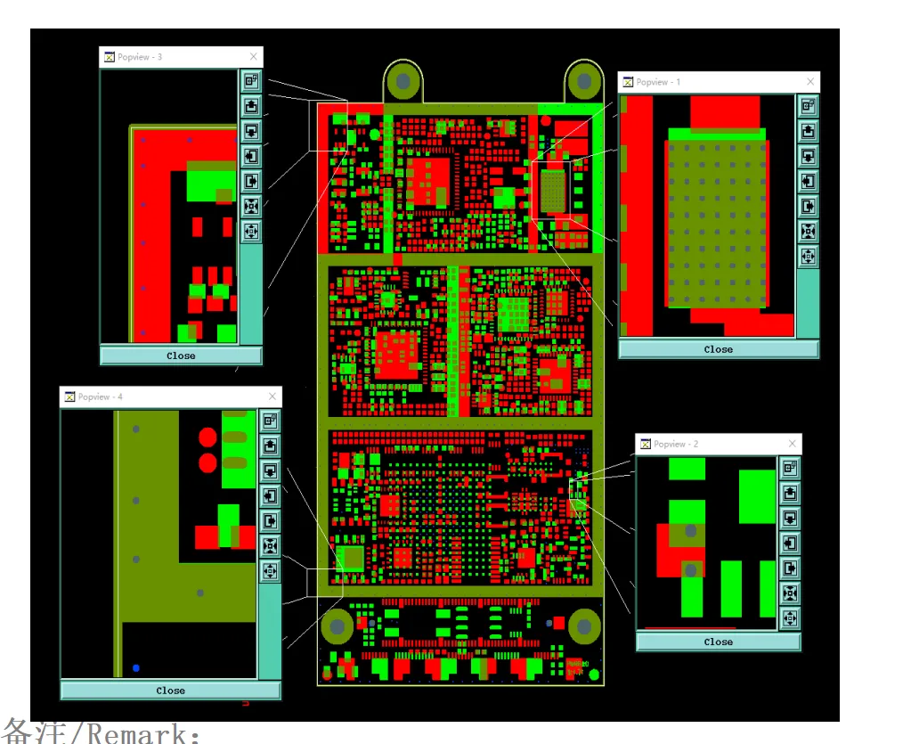
Figure 3: some vias with double-side open window
We recommended following the original Gerber for via windows but highlighted the leakage risk. The customer confirmed to proceed per design, so we documented the decision carefully.
Without clarification, exposed copper around vias after ENIG could lead to tin bridging, corrosion, or assembly defects. NSMD BGA pads without proper support increase the chance of pad lift under mechanical stress.
3. Material Stackup Confirmation
The customer requested Shengyi FR-4 TG150 material, but we did not have the exact matching variant in stock. We prepared a stackup using our standard equivalent FR-4 TG150 halogen-free material and sent the detailed press diagram for approval.
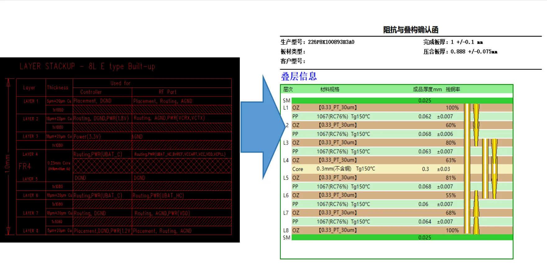
Figure 4: a stackup using our standard equivalent FR-4 TG150 halogen-free material
We noticed this is a frequent occurrence — specified materials often need substitution for lead time and performance matching. After review, the stackup was confirmed.
4. Panelization and Stamp Hole Optimization
The customer provided a panelization PDF. Our team optimized the layout by adding tool holes, optical points, and adjusting stamp hole (mouse bite) positions and bridge widths. The original bridge was too narrow, risking premature board separation and excessive burrs during depanelization.
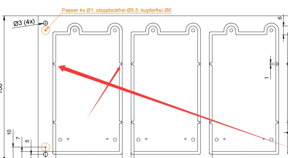
Figure 5: The narrow original bridge
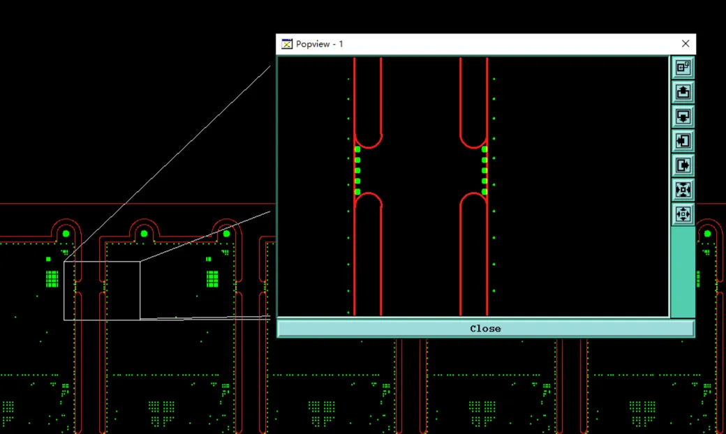
Figure 6: The optimized layout
We sent the revised production panel file for confirmation. Optimizing panelization is critical for production efficiency and final board quality.
Manufacturing Risks and DFM Insights
This case underscores how tight SMD spacing and via mask definitions frequently trigger EQs. Designers often push pad spacing to the limit for routing density without considering solder mask capability, leading to bridge failure. NSMD BGA pads require careful via placement coordination to prevent cratering — a known reliability concern in lead-free assembly.
Panelization details like stamp hole size and bridge width are commonly overlooked, resulting in handling damage or extra manual labor. Material substitution for stackup is standard but always needs confirmation to maintain thickness and registration within tolerance.
How the Engineering Team Resolved the Issues
Our CAM team prepared detailed markup files and comparison images for each issue. After multiple rounds of customer feedback, we finalized solder mask settings, accepted the NSMD BGA as designed with documented risk awareness, confirmed the equivalent material stackup, and optimized the panelization layout with stronger bridges and correct stamp hole positioning.
To reduce manufacturing risk, we also incorporated standard process parameters for ENIG thickness, bow & twist control, and tear-drop allowance on traces.
Final Manufacturing Outcome
All engineering questions were clarified and approved. Production data was updated, DFM review passed, and the order was successfully released for fabrication with optimized panelization and mask parameters.
Key Takeaways for PCB Designers
- Maintain minimum 6 mil solder mask bridge on SMD pads whenever possible to ensure reliable production and assembly yield.
- Clearly define via solder mask strategy (open or tented) consistently across the design to avoid exposed copper risks.
- Consider SMD vs NSMD pad definitions carefully for BGA areas, especially regarding via-in-pad and thermal reliability.
- Provide detailed panelization drawings early and allow factory optimization of stamp holes and bridges for better handling.
- Be open to manufacturer-recommended material equivalents with stackup documentation to avoid delays.
- Include comprehensive process notes (tolerances, markings, bow & twist) in fabrication files to reduce back-and-forth communication.
- Coordinate mechanical features (tooling holes, fiducials) with electrical layout in panelization.
FAQ
Q1: What causes solder mask bridge failure on dense SMD pads?
A1: When pad spacing is below the factory's minimum capability (typically 5.5–6 mil), ink cannot form a reliable bridge, leading to solder shorts during reflow.
Q2: Why are NSMD BGA pads sometimes problematic?
A2: NSMD pads have less mask support around the copper, increasing the risk of pad cratering (pit cracks) under thermal or mechanical stress during assembly and operation.
Q3: Should vias be solder mask open or tented?
A3: It depends on design intent. Open vias risk exposed copper and tin issues after plating; tented vias improve planarity but may trap air. Consistency across the board is critical.
Q4: Why optimize stamp hole positions in panelization?
A4: Poorly placed or narrow bridges cause premature separation, excessive burrs, or board edge damage during depanelization, affecting both yield and cosmetic quality.
Q5: Is material substitution common in PCB production?
A5: Yes. Factories often propose equivalent in-stock materials with matching TG and performance to maintain delivery schedules. Stackup confirmation ensures the final board meets requirements.