










Via in pad design mistakes keep showing up in HDI layouts, especially under fine-pitch BGAs. One wrong call on via treatment and you're looking at solder drainage, voids in the joint, or worse, reliability failures down the road. In 15 years of reviewing these files, the same patterns repeat.
Why Designers Put Vias Directly in Pads
Density drives it. With 0.4mm or tighter BGA pitches, there's simply no room for dogbone fanouts. You drop the via straight under the pad to free up routing channels on inner layers. It shortens signal paths too, which helps with high-speed signals.
But that convenience comes with tight manufacturing tolerances. HDI processes already push limits on microvias, registration, and plating. Skip proper via preparation and the assembly floor pays the price.

Unfilled Vias Creating Solder Wicking Problems
Leaving the via open or only tented is the most common via in pad design mistake I see. During reflow, solder flows down the barrel. You end up with starved joints on the pad surface and excess fillet on the opposite side.
This gets worse with smaller vias. A 0.1mm laser-drilled via has huge capillary action. Even a partial fill leaves enough volume to pull solder away from the component termination.
Typical Failure Mode in Production
X-ray inspection reveals head-in-pillow or incomplete wetting. For BGA packages, this directly impacts electrical continuity and long-term fatigue life under thermal cycling.
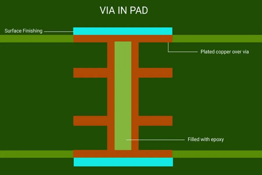
Voids from Incomplete Via Filling
Even when you specify fill, incomplete plugging creates air pockets. Non-conductive epoxy or conductive paste needs proper pressure and multiple passes in many cases. Factories struggle with aspect ratios above 8:1 or inconsistent vacuum.
These voids expand during reflow or in operation, pushing out material or creating delamination. In HDI boards with multiple lamination cycles, trapped volatiles make it even harder to achieve void-free fills.
IPC-4761 Type VII calls for filled and capped vias with specific planarity requirements for SMT attachment. Many via in pad design mistakes ignore the cap plating thickness or planarity tolerance.
Impact on BGA Solder Joint Reliability
A void under the pad reduces the effective contact area. Under CTE mismatch, stress concentrates around the void, accelerating crack propagation. Thermal cycling tests show early failures precisely at these locations.
Pad Size and Annular Ring Considerations in HDI
Pushing pad size too small to fit the via is another frequent issue. You need enough copper for the annular ring after plating and registration tolerances. In HDI, laser via registration can shift 50-75 microns.
IPC-6012 Class 3 typically requires minimum 0.05mm annular ring for reliability. Cut it too close and you risk breakout during drilling or plating defects that trap chemistry.
Soldermask and Surface Finish Interactions
Soldermask defined pads complicate things further. Misalignment between mask, via fill, and cap plating leads to exposed copper or insufficient mask dam between pads. ENIG finish on poorly capped vias can show skip plating or excessive nickel corrosion over time.
These via in pad design mistakes compound in high-volume production where every variable adds up.
Practical Layout Rules to Avoid These Issues
Specify IPC-4761 Type VII for any via-in-pad under SMT components. Call out non-conductive fill for most signal applications and conductive for high current or thermal paths. Require cap plating minimum 12-25 microns depending on class.
- Via diameter: 0.1-0.15mm for 0.4-0.5mm BGA pads
- Pad oversize: ensure at least 0.1mm annular ring after tolerances
- Fill specification: void-free, planar to within 25 microns
- Document fill type and cap requirements clearly on fab notes
Sometimes stepping back to a slightly larger pitch or using staggered microvias gives better yield without sacrificing too much routing. Trade-offs matter.
Long-Term Reliability Observations
Boards that pass initial assembly but fail in the field often trace back to marginal via fills. Vibration or repeated thermal excursions expose weak interfaces. Proper via in pad practices prevent these hidden risks.
Talk to your fab early. Not every shop handles Type VII well on complex HDI builds. Their process capability should drive final design rules more than theoretical minimums.
Key Takeaways for Via in Pad Design Mistakes
Avoid the temptation to treat via-in-pad as just another routing shortcut. Unfilled or poorly filled vias lead directly to solder defects and compromised BGA reliability. Document everything, respect the tolerances, and verify with your manufacturer.
Small adjustments in layout — proper fill calls, adequate pad sizes, clear notes — save far more time than debugging field returns later. That's the practical side of HDI design.






