










When Via-in-Pad Becomes the Only Practical Choice for Dense HDI Layouts
In high-density interconnect boards with fine-pitch BGAs, traditional via routing with dogbone fanouts works well down to about 0.8mm pitch. Below that, especially at 0.5mm and tighter, via in pad vs traditional via shifts heavily toward via-in-pad for maintaining routability. From the fab floor, traditional methods keep costs lower and yields higher on looser designs, while via-in-pad drives up process steps but unlocks routing density that can reduce layer count and overall board size. The decision hinges on your BGA pitch, target layer count, production volume, and reliability requirements rather than a blanket preference.
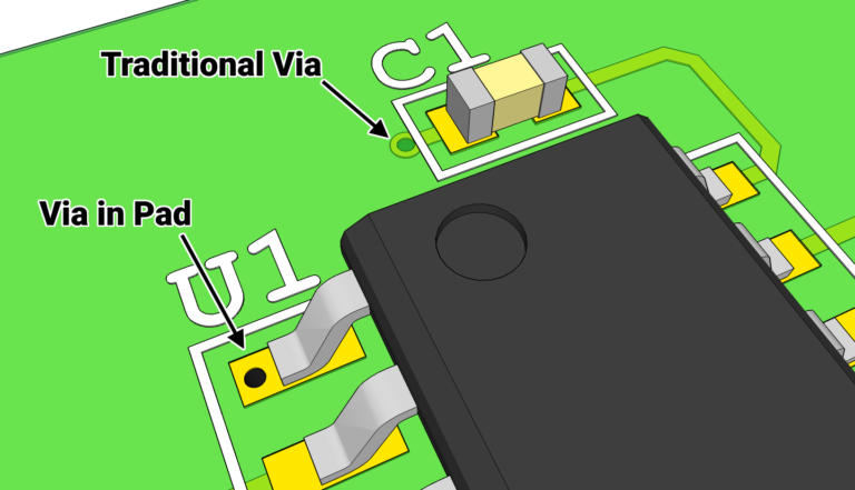
Key Trade-offs at a Glance
| Factor | Traditional Via Routing (Dogbone) | Via-in-Pad |
|---|---|---|
| Cost | Lower baseline; standard processes | 15-30% higher due to filling, planarization, and capping |
| Routing Density / BGA Fanout | Limited below 0.8mm pitch | Excellent for ≤0.5mm pitch; reduces layers needed |
| Manufacturing Complexity | Standard drilling and plating | Additional via fill, cap plating, and surface planarization steps |
| Yield | Higher and more predictable | Lower if fill quality or registration drifts |
| Signal Integrity | Longer traces add inductance | Shorter paths; better for high-speed |
| Reliability | Proven with fewer process risks | Good when properly filled; risk of voids or solder wicking |
| Lead Time | Faster | Extended by extra processing |
Decision Matrix for Via in Pad vs Traditional Via in Production
| Priority | Better Choice | Why from Fab Perspective |
|---|---|---|
| Lowest cost / standard pitch BGAs (≥0.8mm) | Traditional Via Routing | No extra fill or planarization; higher panel utilization and simpler CAM |
| Highest routing density / fine-pitch BGA (<0.5mm) | Via-in-Pad | Eliminates fanout space constraints; often saves layers |
| Fast prototype / quick turnaround | Traditional Via Routing | Fewer process steps mean shorter lead times and easier DFM tweaks |
| High-volume mass production | Depends: Traditional where possible; Via-in-Pad if density demands it | Volume amortizes via-in-pad costs but requires tight process control for yield |
| Best signal integrity / high-speed | Via-in-Pad | Shorter paths reduce inductance; consistent when filled properly |
| Maximum reliability in harsh environments | Traditional Via Routing (with good design) | Fewer variables in plating and fill; lower risk of voids or delamination |
How BGA Fanout Drives the Via in Pad vs Traditional Via Choice
During DFM review, the first thing we check is BGA pitch and row depth. With traditional via routing, dogbone fanouts need space between pads for the trace and via annulus. This works reliably down to 0.8mm pitch but quickly runs out of room on tighter arrays. Signals from inner rows compete for surface routing channels, often forcing extra layers or reroutes.
Via-in-pad places the via directly under the pad, eliminating the fanout trace entirely. This dramatically improves routing density on HDI boards, allowing escape of more signals per layer. In production, we see this reduce stackup thickness and sometimes drop a layer or two, which offsets some of the added via processing cost. However, it demands precise laser drilling (for microvias), reliable filling, and planarization to ensure a flat solderable surface. Any misalignment or incomplete fill shows up fast in assembly as solder wicking or open joints.

Routing Density Differences and When They Matter Most
Traditional via routing preserves more design flexibility on mid-density boards because it uses standard through or blind vias without specialized fill. But in dense HDI with deep BGA arrays, the space consumed by fanouts forces trace necking or additional layers, which increases material usage and lamination cycles. We often see yield drop when designers push traditional methods too far on fine pitch.
Via-in-pad shines here by freeing surface real estate. Factories notice better panel utilization on via-in-pad designs because the board outline can sometimes shrink. The trade-off appears in CAM preparation: more attention to via fill type (conductive vs non-conductive), cap plating thickness, and ensuring no dimples that affect SMT. For high-speed signals, the shorter path in via-in-pad reduces stub effects and improves impedance control compared to longer dogbone routes.
Cost Comparison: Where the Premium Shows Up
Traditional via routing stays cheaper because it follows standard processes—drill, plate, and go. No extra chemistry for filling or additional plating cycles. In volume, this keeps per-board costs predictable and lead times short.
Via-in-pad adds steps: via filling (often with epoxy or conductive paste), planarization to remove excess material, and cap plating for a flat pad. This typically adds 15-30% to bare board cost depending on via count and board complexity. However, if it avoids an extra pair of layers or reduces overall board size, the net cost can break even or improve, especially in mass production. During quoting, we always run both options through CAM to show the real delta.
Reliability and Yield in Real Production Runs
Traditional vias have decades of proven reliability with fewer variables. Solder mask tenting or plugging handles most concerns without risking internal voids. Yield stays high because registration tolerances are looser relative to the process.
Via-in-pad reliability depends heavily on fill quality. Poorly filled vias can trap moisture, cause popcorning during reflow, or create weak solder joints. In our experience, via-in-pad boards require stricter incoming inspection and cross-sectioning during process qualification. Yield tends to decrease initially until process parameters stabilize, particularly on boards with thousands of vias. For high-reliability applications, we recommend conductive fill and thorough thermal cycling validation.
Factory Perspective on Evaluating Via in Pad vs Traditional Via
In CAM engineering, traditional via routing is straightforward—standard drill files, simple plating, and high panel utilization. DFM feedback is usually minor adjustments to clearances. Process stability is excellent with mature equipment.
Via-in-pad triggers more scrutiny: we verify via diameter to pad ratios (typically via ≤80% of pad), confirm fill material compatibility, and simulate planarization results. Tooling costs can rise slightly for specialized fixtures. Production yield depends on laser drill accuracy and plating bath control. We normally recommend via-in-pad only when traditional routing fails DFM or adds layers, and we push for partial implementation (outer rows traditional, inner via-in-pad) to balance risks. Inspection requirements increase—AOI plus sample cross-sections—especially for volume orders. Panel utilization may suffer if via density affects copper balance.
Recommended Figure: Manufacturing process flow comparison chart showing steps for traditional via versus via-in-pad, highlighting added stages and quality checkpoints.
Which Option Should You Choose?
Choose Traditional Via Routing if you:
- Have BGA pitches 0.8mm or larger with manageable routing
- Prioritize lowest cost and fastest lead time for prototypes or medium runs
- Need maximum process simplicity and highest baseline yield
- Operate in applications where signal speeds are moderate
Choose Via-in-Pad if you:
- Face fine-pitch BGAs (0.5mm or below) that cannot route traditionally
- Require maximum density or fewer layers to meet size/weight targets
- Have high-speed signals that benefit from minimal trace length
- Are in volume production where layer reduction justifies the premium
Hybrid approaches often deliver the best results—using via-in-pad selectively for inner BGA rows while keeping traditional routing elsewhere.
FAQs
Q1: Does via in pad vs traditional via always increase overall board cost?
A1: Not necessarily. While via-in-pad adds 15-30% to fabrication cost, it can reduce layer count or board size enough to lower total cost in dense HDI designs. We evaluate this case-by-case during quoting.
Q2: How does pitch affect the choice between via in pad and dogbone fanout?
A2: Above 0.8mm, traditional dogbone is usually sufficient and preferred. At 0.65mm partial via-in-pad may help, but below 0.5mm via-in-pad often becomes mandatory for successful fanout.
Q3: What reliability risks are higher with via-in-pad in HDI PCBs?
A3: Main risks are voids in the fill, solder wicking into the via, and potential delamination under thermal stress. Proper fill material and process control mitigate these effectively.
Q4: Can we mix traditional vias and via-in-pad on the same HDI board?
A4: Yes, and we often recommend it. Use via-in-pad only where density requires it and traditional routing elsewhere to balance cost, yield, and performance.
Q5: How much extra lead time does via-in-pad typically add?
A5: Usually 2-5 days depending on volume and shop load, due to additional filling and inspection steps. Early DFM discussion helps minimize this.






