










Solder Mask Bridge in PCB Manufacturing: Preventing Shorts in Fine-Pitch Designs
WHAT THIS VIDEO COVERS
A solder mask bridge is the narrow strip of solder mask left between adjacent copper pads on a PCB. Its primary function is to act as a physical barrier that prevents molten solder from flowing between pads during reflow, significantly reducing the risk of electrical shorts.
The video covers the key factors that determine minimum bridge width: the PCB fabricator's mask tolerance, solder mask color (green typically allows the finest gaps), copper thickness, and pad spacing. Engineers are shown how to set proper DRC rules early in the design phase and why reviewing the solder mask Gerber layer before fabrication is critical, especially for fine-pitch components such as QFNs and BGAs in HDI and multilayer boards.
These guidelines help teams avoid costly assembly defects when moving from PCB prototype to PCB assembly.
KEY HIGHLIGHTS
- Solder mask bridges create a physical barrier that prevents solder from bridging between fine-pitch pads
- Minimum bridge width depends on fabrication tolerance, solder mask color, and copper thickness
- Reviewing the solder mask Gerber layer before release reduces shorts in QFN, QFP, and BGA assemblies
Understanding Solder Mask Bridges and Their Function in SMT Processes
Solder mask bridges form essential barriers in PCB layouts where component density demands precise control over solder flow. During reflow soldering, molten solder can easily migrate across exposed copper if no physical separation exists, resulting in shorts that compromise circuit functionality. These bridges maintain isolation between pads, supporting consistent joint formation and reducing defects in automated assembly lines.
In practice, the effectiveness of bridges depends on their integration with overall board design, including pad geometry and thermal profiles. For high-volume production, reliable bridges contribute to lower defect rates and streamlined quality control through AOI and X-ray inspection. Without them, even minor variations in paste deposition or placement can lead to bridging, particularly in dense layouts.
Fabrication processes apply the mask after imaging and development, where precise control ensures bridges adhere properly to the substrate and copper features. This step is vital for boards destined for consumer electronics, automotive, or industrial applications where reliability under thermal and mechanical stress is non-negotiable.
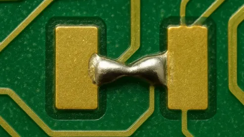
Manufacturing Variables Affecting Solder Mask Bridge Reliability
Several process and material factors influence solder mask bridge performance. Green solder mask typically achieves the narrowest reliable widths around 0.1 mm (4 mil) due to superior resolution and adhesion characteristics, while darker or lighter colors like black and white require wider dimensions (often 5-7 mil) because of differences in ink formulation and exposure behavior. Copper thickness further complicates this, as heavier weights can affect mask flow and edge definition.
Registration tolerances during mask application, typically ±3 to ±5 mil, must be accounted for in design rules to prevent partial coverage or sliver formation. In multilayer and HDI constructions, additional variables such as lamination pressures and material expansion add complexity, potentially stressing narrow bridges.
Designers must evaluate these parameters against specific fabricator capabilities rather than generic guidelines. Failure to do so frequently results in engineering change orders or scrapped panels, increasing lead times and costs.
| Factor | Green Mask Recommendation | Other Colors Recommendation | Impact on Fine-Pitch Designs |
|---|---|---|---|
| Minimum Bridge Width | 4 mil (0.1 mm) | 5-7 mil | Determines feasibility of tight pad spacing |
| Copper Thickness | 1 oz standard | Adjust for 2 oz+ | Affects adhesion and required clearance |
| Registration Tolerance | ±3-4 mil | ±4-5 mil | Critical for maintaining bridge integrity |
Best Practices for Solder Mask Layer Verification Before Production
Thorough verification of the solder mask Gerber file identifies potential issues before committing to fabrication. This includes confirming adequate web widths, proper expansion around pads, and absence of unintended connections or isolated slivers. Tools within CAD software help simulate the manufactured appearance, highlighting risks in fine-pitch areas.
Collaboration with the chosen manufacturer provides tailored DFM feedback, allowing adjustments for their specific processes and equipment. For complex boards, this step often reveals opportunities to optimize panelization or via treatments alongside mask design.
In real production scenarios, skipping detailed review leads to higher rates of post-fabrication corrections or assembly failures. Implementing standardized checklists ensures consistency across projects and supports scalable manufacturing.
Real-World Assembly Challenges with Insufficient Solder Mask Bridges
Insufficient bridge widths commonly manifest as solder shorts in QFN and BGA assemblies, especially when pad pitches approach 0.4-0.5 mm. Production data shows that marginal bridges can detach during handling or reflow, exposing copper and allowing solder to flow freely. This results in immediate electrical failures or latent issues detected only during functional testing or field operation.
Contributing factors include stencil aperture mismatches, aggressive thermal ramps, or board warpage. In thin or high-layer-count boards, these problems compound, leading to reduced yields and increased rework. Case studies frequently highlight the need for proactive design adjustments rather than relying solely on process tweaks at assembly.
Mitigation strategies focus on holistic DFM, including adjusted paste volumes and verified thermal profiles, to complement robust mask design.
Advanced DFM Techniques for Optimizing Solder Mask in Complex Boards
Advanced techniques involve setting comprehensive DRC rules that encompass minimum bridge widths, expansion values, and clearance to traces or vias. For ultra-dense designs, selective use of gang masking combined with precision stencil design offers practical alternatives while maintaining control over solder volume.
Additional considerations include material selection for the mask type and evaluation of long-term reliability under environmental testing. Regular audits of incoming boards against design intent help close feedback loops with fabricators.
These practices enable smoother transitions from prototype to production, minimizing risks in applications requiring high signal integrity and thermal performance.
FAQ
Q1: What is the minimum solder mask bridge width for fine-pitch BGAs?
A1: Most fabricators require at least 0.1 mm (4 mil) between pads, but actual limits depend on the chosen solder mask color and their specific process capability.
Q2: How does solder mask color affect bridge performance?
A2: Green solder mask generally supports the narrowest bridges, while black and white masks often need wider spacing due to lower resolution during imaging.
Q3: Why should engineers review the solder mask Gerber before PCB fabrication?
A3: Reviewing the Gerber ensures bridges are correctly placed and meet the fabricator's minimum tolerances, preventing shorts during SMT assembly.
Q4: What alternatives exist when solder mask bridges cannot be maintained in very fine-pitch layouts?
A4: Gang masking (merged openings) paired with reduced stencil apertures and optimized reflow profiles can control solder flow effectively. This requires close coordination between design, fabrication, and assembly teams, plus enhanced post-reflow inspection.
Q5: How does board thickness or layer count impact solder mask bridge decisions?
A5: Thinner and higher-layer boards experience more warpage and registration challenges, often necessitating conservative bridge widths or additional process controls. DFM reviews should incorporate the full stackup to ensure mask reliability throughout manufacturing.
Have you ever noticed a thin green "wall" between some PCB pads?
It's not decoration — it's a solder mask bridge, and it's more important than it looks.
A solder mask bridge is a narrow strip of solder mask left between pads.
Its job is simple: stop solder from spreading and prevent accidental shorts.
Remove it, and you're much more likely to get solder bridges or shorts, especially on fine-pitch parts like QFPs, QFNs, or BGAs.
How narrow can a solder mask bridge go?
It mainly depends on three things:
Your PCB fab's minimum mask tolerance.
The solder mask color — green usually handles the finest gaps.
The copper thickness and how much spacing your pads have.
So engineers check fab rules early, set proper DRC limits, and always review the solder mask Gerber before sending files.
Want a more stable PCB? Don't overlook the tiny detail of solder mask bridges.
This is aivon, making PCB learning easier, comment below — and follow for more PCB tips!





