When a suspected intermittent connection pointed to a possible soldering issue on an embedded MultiMediaCard (eMMC), non-destructive X-ray inspection was used to evaluate the BGA solder joints beneath the package. The immediate goal was straightforward: assess the solder balls for typical assembly defects such as insufficient wetting, opens, voids, or bridging. While the solder balls appeared uniform and well formed, adjusting the imaging parameters revealed an unexpected internal detail—bond wires and an off-center die within the package.
Why Use X-Ray for eMMC BGA Inspection?
The BGA form factor hides solder joints between the package and the PCB, making optical inspection impossible after reflow. X-ray inspection offers a fast, non-destructive way to assess joint geometry and detect assembly anomalies. For eMMC, this is especially useful because:
- The device integrates NAND flash and a controller in a single package; assembly quality directly impacts system reliability.
- Fine-pitch BGA arrays and high pin counts increase the risk of subtle defects that are not electrically obvious immediately after assembly.
- Mechanical warpage of thin substrates during reflow can contribute to non-wet opens that X-ray can often reveal.
Typical BGA issues that X-ray can help identify include:
- Insufficient wetting (non-wet opens) or "head-in-pillow" conditions that result from warpage or reflow profile mismatches.
- Excessive voiding within the solder joint, which can compromise mechanical or thermal performance.
- Solder bridges or shorts between adjacent balls.
- Ball-to-pad misalignment or insufficient collapse indicating poor wetting or misplaced components.
Initial Assessment: Solder Balls Look Healthy
Top-down X-ray images showed the BGA array with consistent grayscale intensity and geometry across the field. The solder balls appeared "full and even," indicating uniform collapse and wetting to the PCB pads. No obvious bridging, excessive voiding, or asymmetry in ball size was evident. This type of uniformity suggests that the stencil, paste application, placement accuracy, and reflow parameters were all within acceptable bounds for the given assembly process.
The absence of obvious defects in the joints narrowed the likely root causes of the original intermittent issue. In practice, that often shifts attention to other contributors such as board-level warpage under thermal or mechanical stress, localized PCB pad contamination, or downstream handling issues. However, before drawing conclusions, a deeper pass with the X-ray system was performed.
Tuning the Image: Internal Bond Wires Come Into View
By adjusting the imaging setup—effectively changing penetration and focal conditions—the inspection revealed internal wire bonds within the eMMC package. These fine bond wires connect the die to the package substrate and are visible under certain X-ray settings, especially when laminography or oblique-angle views are used to de-emphasize the solder balls and bring internal structures into focus.
Interestingly, the bond wires appeared concentrated on one side of the package, and the opposite side showed no visible wire connections. This indicates the active die is positioned off-center within the package footprint. The observation suggests that only one die site is populated and bonded in this specific device.
Interpreting the Off-Center Die
An off-center die inside a standard-size package is not unusual and does not imply a defect. Several design and manufacturing considerations can lead to this layout:
- Package family reuse: The same package outline may be used for multiple density options. Higher-capacity parts can populate additional die sites or stack dies, while lower-capacity parts may use a single die placed at one location on the substrate.
- Wire-bond routing optimization: Die placement can be offset to simplify bond wire routing or minimize parasitic inductance for critical signals between the NAND array and the controller within the package.
- Thermal and mechanical considerations: Die placement and bond patterns are part of an overall package design that balances thermal expansion, stress, and manufacturability.
In eMMC, it’s common for the package to integrate at least two functions—NAND storage and a controller—as either separate dies or integrated differently depending on the vendor and density. For a modest-capacity part, a single NAND die may be populated, and the remaining area inside the package remains unoccupied. The X-ray result in this case is consistent with a single-die configuration.
Practical Checklist for eMMC BGA X-Ray Review
When performing X-ray inspection on eMMC BGA packages, a structured checklist helps ensure meaningful conclusions:
- Ball uniformity: Check for consistent ball size, shape, and grayscale intensity across the array. Significant variation can indicate paste volume issues, partial wetting, or process variation.
- Collapse and alignment: Confirm that balls have collapsed consistently and are well centered on the pads. Off-center balls can indicate placement error or pad misregistration.
- Voiding: Evaluate the presence and distribution of voids within individual joints. A few small voids are typically benign; extensive or large voids may reduce mechanical strength or affect heat conduction.
- Bridging and opens: Look for evidence of solder connections between adjacent balls or balls that failed to connect to their pads. "Head-in-pillow" often appears as a separation plane or uneven grayscale within the ball.
- Peripheral anomalies: Pay attention to edge balls, where warpage-induced non-wet opens are more likely during reflow.
- Internal structures: When needed, adjust imaging to examine internal features such as bond wires. Use caution interpreting internal features, as 2D X-ray can superimpose structures; laminography or CT can improve separation.
Manufacturing Considerations Behind Common Findings
Several upstream design and process factors strongly influence what X-ray reveals:
- Pad design: Solder mask defined (SMD) versus non-solder mask defined (NSMD) pads affect solder spread and joint geometry. NSMD pads typically yield more consistent wetting and collapse, which often appears as smoother grayscale in X-ray images.
- Stencil and paste: Aperture design and paste volume uniformity directly affect ball collapse. Inconsistent paste volume can manifest as a mosaic of brighter/darker balls or unusual ball geometry in X-ray.
- Reflow profile: Ramp, soak, and time-above-liquidus influence wetting and void evolution. Profiles that are too aggressive or too mild can promote void entrapment or insufficient intermetallic formation.
- Warpage control: Thin packages and boards can bow during reflow. If the package lifts off pads at peak temperature, non-wet open joints or head-in-pillow defects can result—often visible in X-ray post-reflow.
- Board support and fixturing: Proper support during reflow helps reduce dynamic warpage and improves joint integrity, especially for large packages or thin PCBs.
Limitations of X-Ray and Complementary Methods
While X-ray is a powerful tool, it has limitations and should be interpreted in context:
- Metallurgical details: X-ray shows geometry and density variations but does not directly reveal intermetallic layer quality or micro-cracks at the interface.
- Superposition: 2D X-ray projects multiple layers into one image. Internal structures can overlap, making interpretation challenging. Laminography or CT-based methods can isolate layers but require more time and equipment capability.
- Delamination and voiding beyond solder joints: For internal delamination within the package or voiding in underfill/encapsulants, scanning acoustic microscopy (SAM) can be a better diagnostic tool.
- Functional correlation: A clean X-ray image does not guarantee long-term reliability. If failures persist, correlate X-ray findings with electrical tests, thermal cycling results, and, if necessary, destructive analysis.
Observational Summary and Takeaways
In this inspection, the BGA solder joints appeared healthy: consistent ball geometry, no obvious bridging, and no significant voiding were observed. Adjusting the X-ray focus to examine internal structures revealed bond wires and indicated that the die is positioned off-center within the package. This is consistent with a single populated die site in a package family that may support multiple configurations across different storage capacities.
For PCB designers and manufacturing engineers, the exercise reinforces a few practical points:
- X-ray is an effective first-line tool to confirm solder joint integrity on BGAs like eMMC, especially when failures suggest assembly issues.
- Interpreting internal features requires awareness of package design; off-center die placement is not inherently abnormal.
- If solder joints look clean but failures persist, consider warpage management, pad design, and process control, and be prepared to use complementary methods for deeper analysis.
Non-destructive imaging remains a cornerstone diagnostic for modern electronics assemblies. Used thoughtfully, it not only validates solder joint quality but can also provide insight into package construction—occasionally revealing unexpected but perfectly benign details inside the device.

Figure 1 | Top-down X-ray view of the eMMC BGA showing a uniform solder ball array.
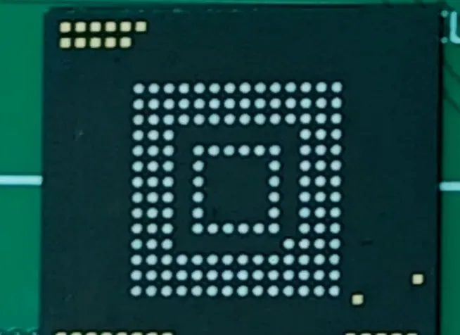
Figure 2 | Magnified region highlighting consistent grayscale and ball geometry.
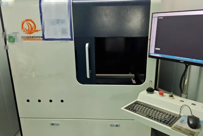
Figure 3 | Alignment and collapse appear consistent across the array.

Figure 4 | Central region detail with no bridging or opens observed.

Figure 5 | Solder balls appear full and even, indicating good wetting.

Figure 6 | Peripheral rows show the same uniformity as interior rows.
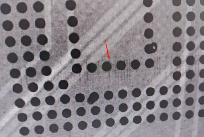
Figure 7 | Bond wires inside the eMMC package become visible.
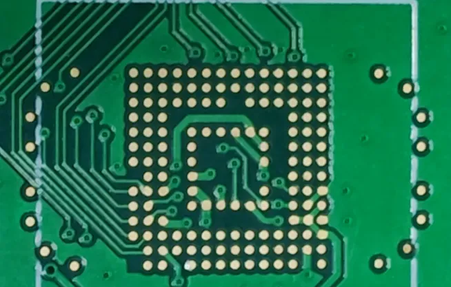
Figure 8 | Close-up of bond wire routing connecting the die to the substrate.
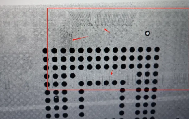
Figure 9 | Evidence of off-center die placement—bond wires are present on one side only.