DFM (Design for Manufacturing) and DFA (Design for Assembly) aim to align product design with manufacturing and assembly capabilities. Without practical manufacturability analysis before fabrication, latent design issues often flow downstream into production, driving repeated back-and-forth, lowering yield, and extending development cycles. Robust DFM checks are therefore critical.
- From a product perspective: reduce the number of design spins and integrate physical design practices with actual manufacturing equipment capability.
- From a development methodology perspective: adopt concurrent engineering to achieve first-pass success from design to manufacturing.
- From a business perspective: improve efficiency, shorten schedules, reduce cost, and meet high-reliability product requirements.

Open/Short Analysis
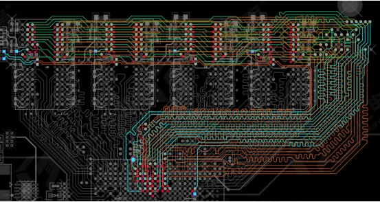
Use the PCB fabrication data as the basis and compare the software-extracted nets against the actual physical connectivity on the PCB. Analyze opens and shorts in a physically meaningful way and perform multi-dimensional checks to catch critical, design-breaking issues before fabrication.
Electrical Signal Checks
- Right-angle and sharp-angle traces introduce abrupt changes in signal direction, which causes reflections and transmission discontinuities that can degrade signal integrity.
- In fabrication, right-angle and sharp-angle corners can trap etchant (often referred to as "acid traps"), leading to uneven etching and reduced conductor width at corners, which further impairs signal continuity.
- Use 45-degree miters or rounded corners for trace bends. For T-branches that cannot be avoided, add teardrops to reinforce the connection mechanically and electrically at the junction.
Trace Width and Spacing Checks
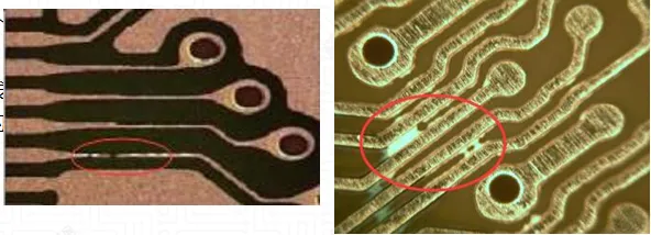
- Trace width is directly related to current-carrying capability—narrower traces carry less current. For multiple high-speed lines routed in parallel over long distances, follow the 3W principle to manage coupling and crosstalk.
- Select manufacturing capability commensurate with your design rules to avoid yield risks from width/spacing limits. For example, narrow traces are more susceptible to over-etching and potential opens; tight spacing increases the risk of resist residue or incomplete etching between lines, leading to shorts.
Annular Ring Size Checks
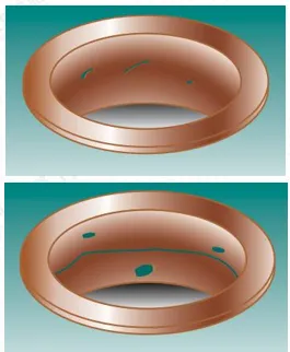
- Small annular rings reduce pad adhesion and mechanical robustness. During soldering or rework, pads can detach, and smaller solderable areas on through-hole pins can reduce solder joint reliability. Increasing the annular ring, where space allows, improves product robustness.
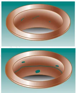
- Manufacturing tolerances on hole position and drill wander can further reduce the effective annular ring. Rings that are too small risk breakout, compromising conductive reliability, as shown in the figure.
Vias in SMD Pads
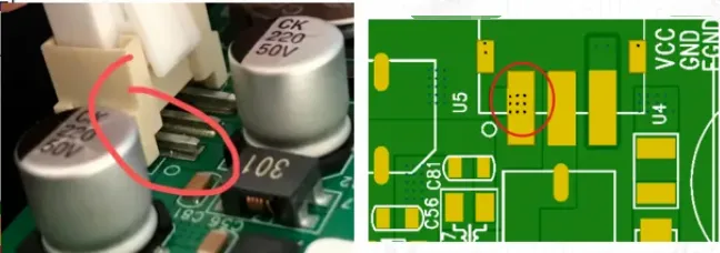
Vias placed within SMD pads (often called via-in-pad or "hole-on-pad") create depressions that disturb planarity and can draw solder away during reflow, harming solder joint quality. To ensure reliable assembly, such holes typically require filling and plating to create a flat, solderable surface—raising fabrication cost. Where layout space permits, avoid vias in SMD pads to reduce cost and prevent defects such as insufficient solder or voiding, as illustrated.
Drill Diameter Checks
- The minimum practical mechanical drill size commonly used is around 0.15 mm. Holes smaller than 0.15 mm typically require laser drilling, which costs significantly more. Even within mechanical drilling, smaller diameters drive higher cost.
- For plated through vias, consider the aspect ratio (board thickness to hole diameter). At diameters below 0.2 mm, plating solution throwing power degrades, increasing the risk of voids or cracks in the copper barrel. Chemical processes, including desmear and electroplating, can further stress small vias. To mitigate via-related defects, design via diameters ≥ 0.2 mm where possible (0.3 mm is often a robust target), as shown.
Hole-to-Hole Spacing (Fabrication Checks)
- Insufficient spacing between holes degrades yield. During drilling, inadequate pitch can increase drill-bit breakage.
- When holes belonging to different nets are too close, conductive anodic filament (CAF) growth and electrical shorting risks increase.
- For through-hole component pins with tight hole spacing, solder bridging is more likely during wave soldering or hand soldering, as shown in the figures.

Special Hole Checks
- Rectangular and square holes pose data-format and toolpath constraints: CNC drill data cannot form true internal right angles. CAM tools at the board house may interpret these as circular or oval apertures.
- If rectangular or square non-plated cutouts are required, define them in the outline/mechanical layer and coordinate with the fabricator to ensure the intended shape and tolerances.
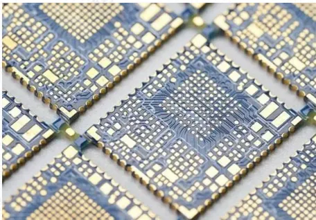
- Castellated or half-plated holes (so-called "stamp holes") are metalized holes cut at the board edge. They require special process steps and notes to the fabricator to ensure proper half-plating and edge quality, as illustrated.
Solder Mask Dam (Solder Mask Bridge) Checks
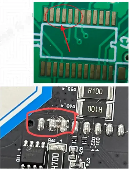
- A solder mask dam (also called a solder mask bridge) provides an isolation band between SMD pads to prevent solder bridging during reflow. It reduces the risk of shorts between fine-pitch leads. Typical manufacturing capabilities for minimum solder mask dam width are about 4 mil for green, 5 mil for black, and around 4.5 mil for other colors. When defining component footprints, consider pad-to-pad spacing. If pad spacing approaches 6 mil or less, apply appropriate mask compensation and optimize pad geometry to maintain at least about 6 mil clearance between exposed pads.
- Lack of solder mask dams significantly increases the risk of solder bridging, as shown in the examples.
Missing Solder Mask Checks
- Solder mask defines the non-solderable regions ("covered by ink"). Openings in the mask define solderable areas for components. If openings are missing or too small, pads may be covered by mask, preventing proper soldering.
- Typical causes include footprint definition errors and missing mask openings during Gerber data generation. Validate mask openings during design handoff to avoid assembly issues, as shown.