8-layer impedance boards with tight 6mil features and BGA areas are particularly prone to DFM issues during CAM review. This real engineering case examines an 8-layer FR-4 design that required multiple clarifications before production. As a senior CAM engineer with over 15 years of experience, I frequently handle cases where electrical requirements in the notes do not fully align with the actual Gerber data.
This project highlighted common gaps between design intent and manufacturing reality, especially around impedance documentation, stackup consistency, and solder mask treatment in dense BGA regions. The following details the key issues we identified and resolved.
Order Overview
This was an 8-layer FR-4 PCB using TG150 material from KB with a finished thickness of 1.6mm and 1oz copper throughout. Minimum hole size was 0.3mm with 6mil line/space. Surface finish was ENIG, green solder mask, and white silkscreen. The design specified impedance control with report, 100% flying probe testing, and resin plugging for certain vias. Panelization was 1x1 with 6mm process edges. Quantity was 50 pieces (50 sets).
While the parameters looked relatively standard for a controlled impedance multilayer board, the combination of specific impedance targets, BGA layout, and incomplete reference data created several manufacturability concerns that our CAM team had to address before releasing the files.
Main Engineering Questions Found During CAM Review
Stackup Thickness Mismatch and Impedance Reference Issues
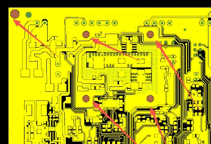
The customer's processing notes specified a board thickness that did not match the provided stackup drawing. More critically, we could not locate the required 85ohm differential lines in the actual files. Layer 6 also lacked the expected 50ohm and 100ohm reference traces.
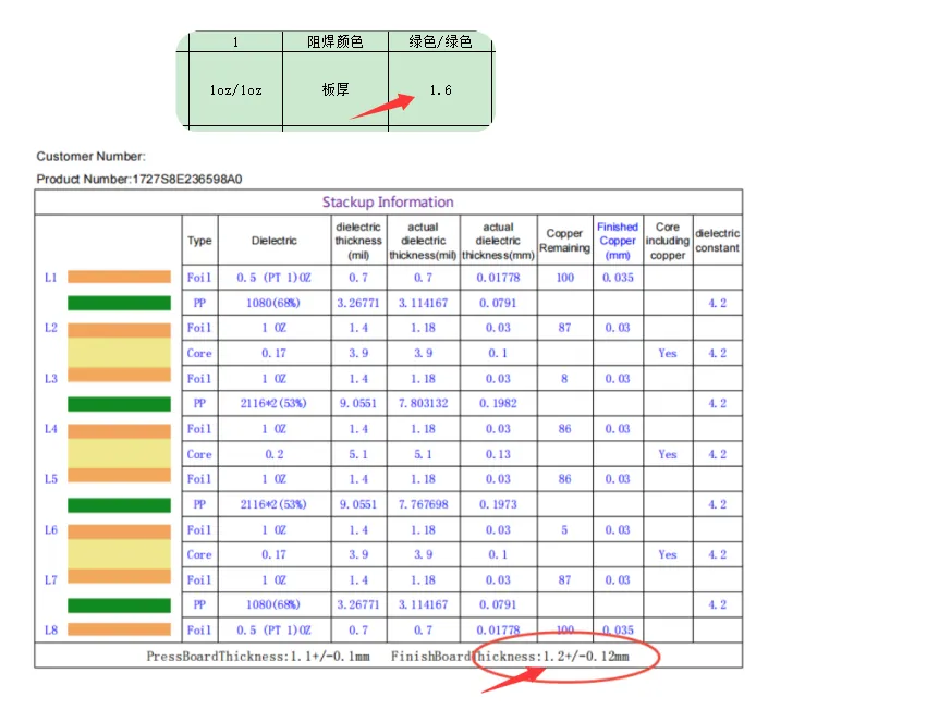
Figure 1: board thickness that did not match the provided stackup
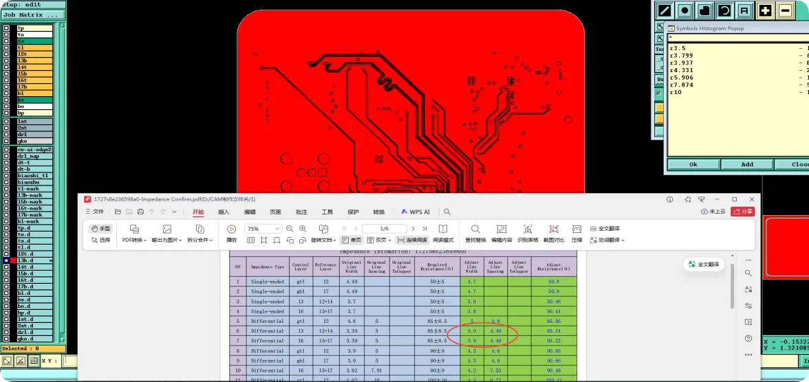
Figure 2: layer 6 lacked the expected 50ohm and 100ohm reference traces
We noticed this immediately during impedance modeling. Our engineer recommended adjusting trace widths and confirming the final stackup to achieve the primary targets. Some impedance lines also lacked complete shielding on reference layers, which could cause distortion in finished impedance values. According to IPC-2221 guidelines, proper reference planes and trace geometry are essential for consistent controlled impedance.
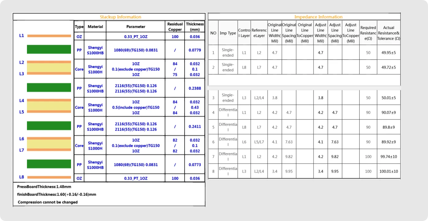
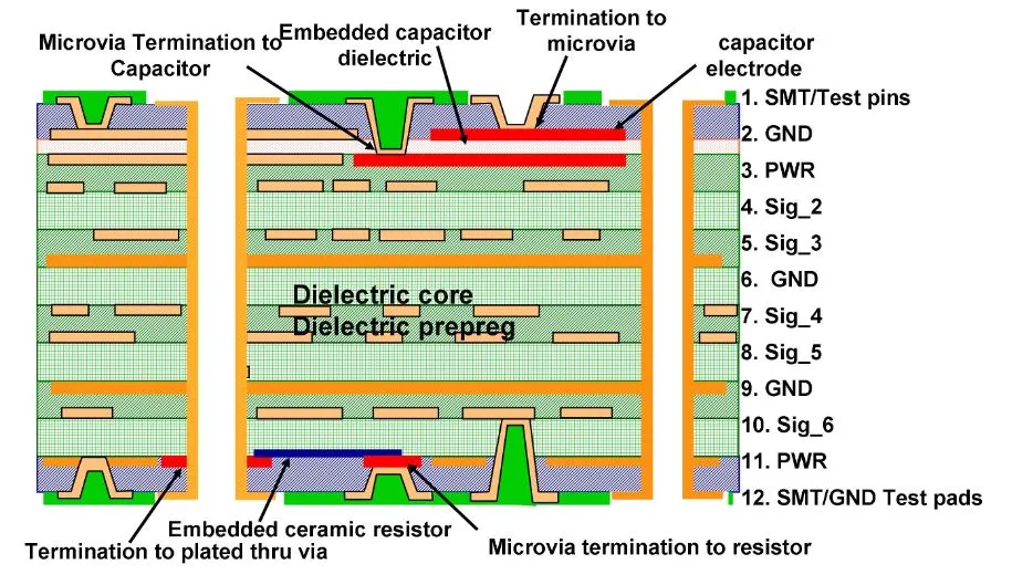
Figure 3: PCB stackup and impedance
If we had ignored these discrepancies, the boards would likely have failed impedance testing, leading to signal integrity problems such as reflections, crosstalk, or timing failures in the end product. We have seen similar unaddressed cases result in full lot rejection after electrical validation.
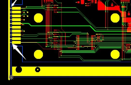
BGA Area Solder Mask Via Openings and Bridge Risks
Several vias in the BGA region had solder mask openings on both sides. This created two issues: increased risk of solder bridging (short circuits) during assembly and insufficient mask bridges between nearby IC pads due to tight spacing.
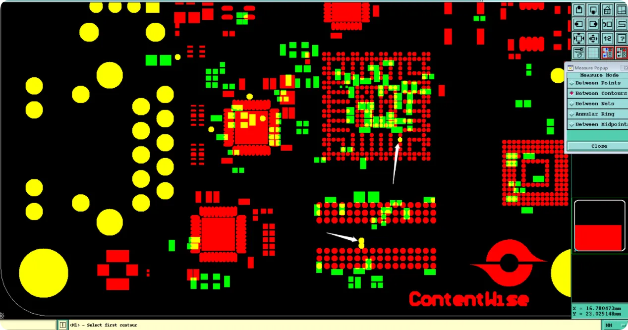
Figure 4: several vias in the BGA region had solder mask openings on both sides
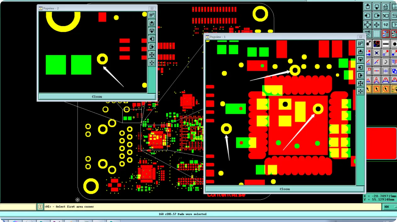
Figure 5: BGA area solder mask via openings
Our CAM team identified this during solder mask data review. We flagged it because via openings in dense BGA areas commonly cause assembly defects. If ignored, excess solder could wick into the vias or create shorts between pads, leading to assembly failures, rework, or functional defects. The customer confirmed handling instructions for these features.
Tight Line/Space Copper Bridge Removal
Due to the relatively tight line/space in some areas, small copper bridges remained between pads after initial processing. We proposed optimizing and removing these isolated features to prevent short circuits during etching and plating.
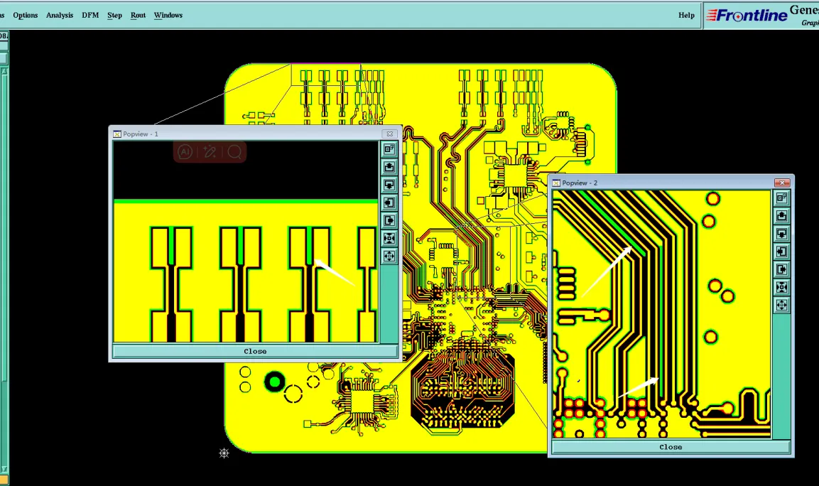
Figure 6: tight line/space in some areas
We noticed this while preparing production files. Removing such bridges is a standard DFM practice on finer geometries to maintain yield. Proceeding without optimization could have caused multiple short circuits and significant scrap.
Other Clarifications
Additional points included silkscreen character thickness (risk of blurring), addition of production markings and UL identifiers, panelization confirmation, and minor impedance line width variations (1-2ohm difference after adjustment).
Figure 7: large silkscreen character
Manufacturing Risks and DFM Insights
This case illustrates typical challenges in 8-layer impedance designs: incomplete reference trace documentation, stackup inconsistencies, and solder mask decisions in BGA zones. Designers often place impedance requirements in notes without ensuring matching geometries in the Gerber files, and via mask treatments in dense areas are frequently overlooked.
If left unclarified, these issues commonly lead to impedance deviation, solder bridging, short circuits, and assembly yield loss. In one comparable project, unaddressed BGA via openings caused widespread solder shorts and required a full respin.
How the Engineering Team Resolved the Issues
Our team prepared detailed markups and calculation reports showing the missing traces and proposed adjustments. We suggested stackup alignment and trace optimization to meet the main impedance targets. For the BGA vias, we confirmed acceptable mask opening strategy with the customer to balance via protection and solder mask bridging.
We noticed the copper bridges early and optimized them in the production files. All changes, including silkscreen adjustments and panel confirmation, were documented and approved before final output. This proactive workflow prevented production delays.
Final Manufacturing Outcome
All engineering questions received customer confirmation. Production files were updated with aligned stackup, optimized impedance geometry, adjusted solder mask treatment, and cleaned copper features. The order was approved for fabrication with enhanced manufacturability.
Key Takeaways for PCB Designers
- Always include actual reference traces matching your impedance targets directly in the Gerber files rather than relying solely on notes.
- Ensure stackup drawings and order specifications are consistent regarding finished board thickness.
- Carefully review via solder mask openings in BGA regions to avoid solder wicking and bridging risks.
- Allow reasonable DFM optimization for small copper islands or bridges in tight line/space areas.
- Verify that impedance lines have proper reference plane shielding on adjacent layers.
- Design silkscreen features with sufficient clearance from pads and consider standard ink thickness limits.
- Provide complete, up-to-date production files and clearly communicate allowable adjustments for impedance.
FAQ
Q1: Why are missing impedance reference traces a common problem?
A1: Notes often specify targets without corresponding geometries in the design files, forcing factories to recalculate or adjust, which may shift final values.
Q2: What risks do via mask openings create in BGA areas?
A2: Solder can wick into vias or bridge to nearby pads during reflow, causing shorts and assembly defects. Selective plugging or mask coverage is often preferred.
Q3: Why do factories sometimes remove small copper bridges?
A3: In tight geometries, these bridges can cause etching shorts or plating defects. Removing them improves yield and reliability.
Q4: How important is stackup consistency with order specifications?
A4: Mismatches can affect impedance, registration, and overall board performance. Alignment early in CAM review prevents costly revisions.
Q5: Can impedance values be slightly adjusted during production?
A5: Minor optimizations (1-2 ohms) are often necessary due to material variations. Prioritizing primary targets ensures the board functions as intended.