










SMD vs NSMD PCB Pads: Critical Differences for Reliable SMT Assembly
What This Video Covers
This video explains the critical differences between SMD and NSMD pads and why the choice directly impacts solder joint reliability in PCB fabrication and SMT assembly.
NSMD pads feature a mask opening larger than the copper pad, fully exposing the copper edges for maximum wetting area and easier post-assembly inspection. SMD pads have the solder mask overlapping the pad edges, which defines a smaller effective soldering area for tighter control in high-density layouts.
Key engineering considerations include pitch size, mask alignment tolerance, and solder volume control. NSMD is typically preferred for standard-pitch BGAs due to superior wetting and reliability, while SMD often performs better in fine-pitch ICs and micro BGAs where mask dams can become too narrow and risk bridging or breakage.
The decision affects signal integrity, thermal management, and long-term mechanical stress in applications ranging from consumer electronics PCB to medical devices PCB and automotive PCB. Viewers will gain practical guidelines to reduce defects and improve yield during PCB prototype and PCB mass production.
Whether you're designing HDI boards or planning PCB assembly, understanding SMD vs NSMD helps avoid costly revisions and ensures robust manufacturing outcomes.
KEY HIGHLIGHTS
- NSMD pads maximize wetting area and inspection visibility but risk solder bridging in fine-pitch designs due to narrow mask dams.
- SMD pads provide better control and density for micro BGAs and fine-pitch components by defining a precise solder area, though they reduce overall wetting.
- Selection depends on pitch, mask tolerance, and application — NSMD is the default for most standard designs, while SMD excels in high-density, reliability-critical layouts.
Understanding SMD and NSMD Pad Structures
SMD (Solder Mask Defined) pads have the solder mask layer overlapping the edges of the copper pad, creating a well-defined solderable area that is smaller than the full copper footprint. This overlap helps contain solder paste during stencil printing and reflow, providing precise control over the solder joint geometry.
In contrast, NSMD (Non-Solder Mask Defined) pads expose the entire copper pad with the mask opening larger than the pad itself. This configuration allows solder to wet the top and sides of the copper, increasing the effective contact area and improving mechanical strength of the joint.
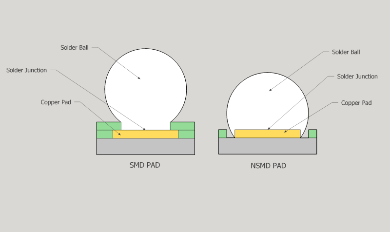
Production data from high-volume SMT lines shows that NSMD pads generally achieve better fillet formation and higher pull strength in standard applications, while SMD pads excel when registration tolerances are tight and pad spacing is minimal.
Solder Joint Reliability and Manufacturing Performance
The choice between SMD and NSMD directly influences thermal cycling performance, mechanical shock resistance, and long-term reliability under operational stress. NSMD pads offer superior wetting, which reduces voiding and enhances heat dissipation, particularly beneficial for power components and BGAs in automotive electronics.
However, in fine-pitch scenarios below 0.5 mm, the reduced mask dam width in NSMD designs can lead to solder bridging during reflow, especially if paste volume is not tightly controlled or if mask alignment deviates. SMD pads mitigate this by providing physical barriers that contain solder spread.
Real-world manufacturing scenarios demonstrate that improper pad selection can increase defect rates by 2-5x in dense layouts, leading to higher rework costs and potential field failures in mission-critical applications such as medical devices.
DFM Best Practices for High-Density and Fine-Pitch Designs
Effective DFM for SMD vs NSMD requires close collaboration between designers and fabricators to evaluate pitch, component footprint, and process capabilities. For standard-pitch BGAs (0.8 mm and above), NSMD is often the preferred choice to maximize reliability margins.
In micro BGA and fine-pitch QFN packages, SMD pads allow narrower mask dams to be avoided, reducing the risk of mask damage during handling and improving yield in high-density HDI boards. Designers should specify mask clearance tolerances of 50-75 µm for NSMD and verify solder mask registration accuracy with the manufacturer.
Additional recommendations include optimizing stencil aperture ratios, adjusting paste volume per pad type, and conducting design rule checks (DRC) that account for both pad geometry and assembly process windows. These practices help minimize tombstoning, head-in-pillow defects, and non-wet opens in volume production.
Common Defects and Mitigation Strategies
| Aspect | SMD Pads | NSMD Pads | Recommended Use Case |
|---|---|---|---|
| Wetting Area | Smaller, controlled | Larger, full copper exposure | NSMD for standard pitch |
| Bridging Risk | Lower in fine-pitch | Higher if dams are narrow | SMD for <0.5 mm pitch |
| Inspection | More challenging | Easier visual access | NSMD for prototypes |
| Mechanical Strength | Good with proper fillet | Generally superior | NSMD for high vibration environments |
| Mask Alignment Sensitivity | Lower impact on joint | Higher due to exposed edges | SMD in tight tolerance processes |
Common failure modes include mask dam breakage in NSMD fine-pitch arrays and insufficient wetting on SMD pads under high thermal loads. Mitigation involves iterative design reviews, prototype builds with X-ray inspection, and statistical process control on solder paste deposition.
FAQ
Q1: What is the main risk of using NSMD pads in fine-pitch PCB designs?
A1: The primary risk is solder bridging when mask dams become too narrow or break, especially in high-density or misaligned processes.
Q2: When should engineers choose SMD pads over NSMD for BGA components?
A2: Choose SMD for fine-pitch ICs and micro BGAs where tighter solder control and reduced bridging risk outweigh the smaller wetting area.
Q3: Does the choice between SMD and NSMD affect PCB assembly cost or reliability?
A3: Yes — the wrong choice can increase defect rates, rework, and field failures, directly impacting reliability and total cost in PCB assembly and volume production.
Q4: How does solder mask registration tolerance influence SMD vs NSMD pad performance?
A4: Tight registration is more critical for NSMD pads because any misalignment can expose unintended copper or reduce the effective dam width, leading to shorts or opens. Fabricators typically recommend reviewing tolerances during the quoting stage for high-density designs.
Q5: Are there specific applications where NSMD pads are strongly preferred?
A5: NSMD pads are preferred in automotive, industrial, and high-reliability applications requiring maximum mechanical strength and thermal performance, provided pitch allows sufficient mask dam width. Always validate with assembly trials.
How do you decide between SMD and NSMD pads?
They are not interchangeable.
And the wrong choice can directly affect solder reliability.
NSMD means the mask opening is larger than the pad, exposing copper edges.
SMD means the mask overlaps the pad and defines the effective area.
Here's the risk.
NSMD can cause bridging when solder mask dams become too narrow or break in fine-pitch designs.
SMD reduces wetting area and can increase stress at the pad edge.
So how do you choose?
It depends on pitch, mask alignment tolerance, and solder control.
For standard pitch BGAs, NSMD is preferred.
For fine-pitch ICs or micro BGAs, SMD is more reliable.
NSMD is the default for wetting and inspection.
SMD is the solution for density and control.





