Introduction
Printed circuit boards form the backbone of electronic systems, and electric engineers often encounter damaged traces and pads during prototyping, assembly, or field service. These issues can disrupt signal integrity, cause short circuits, or lead to complete board failure if not addressed promptly. Precision tools enable targeted PCB trace repair and PCB pad repair, minimizing downtime and preserving costly prototypes. This article explores proven soldering techniques and methods using a rework station or PCB repair kit to achieve reliable fixes. By mastering trace reconstruction, pad replacement, and via repair, engineers can extend board life and maintain performance standards. Understanding these techniques ensures compliance with industry benchmarks for rework quality.
Why PCB Trace and Pad Damage Matters in Engineering Workflows
Traces carry electrical signals between components, while pads provide mechanical and electrical connections for soldering leads. Damage to either compromises functionality, especially in high-density boards where space is limited. For electric engineers, unrepaired defects lead to iterative redesigns, increased costs, and delayed product launches. IPC-7711/7721 outlines criteria for acceptable rework, emphasizing the need for repairs that match original electrical and thermal properties. Precision interventions prevent propagation of faults, such as intermittent connections from cracked traces. Ultimately, effective PCB repair maintains system reliability in demanding applications like power electronics or RF circuits.
Common Causes of Trace and Pad Damage
Mechanical stress from mishandling, probing, or thermal cycling often fractures fine traces, particularly on flex or high-layer-count boards. Overheating during soldering or component removal lifts pads due to differential expansion between copper and substrate. Environmental factors, including humidity and vibration, accelerate degradation over time. Poor initial fabrication, like inadequate copper adhesion, exacerbates these issues under operational loads. Engineers must identify root causes through visual inspection and continuity testing to select appropriate PCB trace repair or PCB pad repair strategies. Prevention aligns with J-STD-001 requirements for soldering processes that minimize heat exposure.
Technical Principles Behind Effective Repairs
Successful PCB repair relies on matching the original trace width, thickness, and impedance to avoid signal distortion. Copper foil repairs must adhere firmly without introducing voids, using adhesives compatible with FR-4 substrates. Thermal management is critical; excessive heat warps boards or delaminates layers during pad replacement. Conductive epoxies provide low-resistance paths for trace reconstruction but require curing profiles to achieve stable conductivity. Vias, acting as interlayer connections, demand precise drilling and plating to restore barrel integrity. These principles ensure repairs withstand environmental stresses per IPC standards.
Essential Tools for Precision PCB Repair
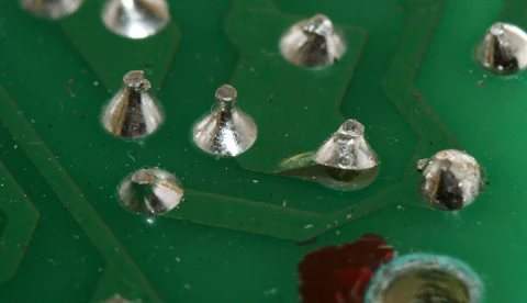
A rework station serves as the core setup, combining hot air, infrared heating, and magnification for controlled operations. Fine-tip soldering irons with temperature regulation enable pinpoint heating for delicate soldering techniques. A PCB repair kit typically includes wire jumpers, eyelets, conductive pens, and Kapton tape for insulation. Microscopes or magnifiers reveal microcracks invisible to the naked eye, guiding accurate interventions. Multimeters and oscilloscopes verify post-repair continuity and signal quality. Selecting tools with adjustable airflow prevents collateral damage to adjacent components.
Step-by-Step PCB Trace Repair Techniques
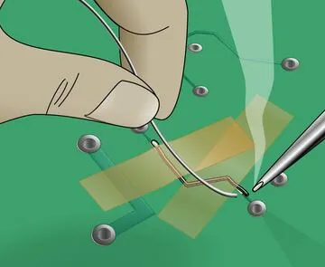
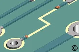
Begin PCB trace repair by cleaning the damaged area with isopropyl alcohol and a soft brush to remove oxidation. For minor fractures, apply conductive silver epoxy along the break, bridging with a thin wire if needed for strength. Cure the epoxy per manufacturer guidelines, typically at room temperature or low heat, then insulate with polyimide tape. In cases of extensive damage, excise the faulty section and install an insulated jumper wire soldered at both ends, matching original trace gauge. Test resistance to ensure it falls within 10% of specification. This trace reconstruction method preserves multilayer integrity without full board replacement.
For wider traces, adhesive-backed copper foil offers a robust alternative. Cut the foil to match the trace dimensions, apply flux, and solder in place using a drag soldering technique. Smooth the surface with a fiberglass brush to remove excess flux residue. Verify with a four-point probe for uniform conductivity. These soldering techniques, executed via a rework station, align with best practices for minimal thermal stress.
Advanced PCB Pad Repair Methods
Lifted pads require immediate PCB pad repair to restore solderability. For small lifts, tenting with epoxy and embedding an eyelet provides mechanical support. Drill a precise hole through the pad site, insert a plated eyelet, and flare it using a hand tool for secure fit. Solder the component lead directly to the eyelet, ensuring fillet formation per J-STD-001. This pad replacement technique suits single-sided boards effectively.
On multilayer boards, donor pad replacement involves bonding a pre-cut copper pad from scrap material. Align under magnification, apply conductive adhesive, and reflow with hot air from a rework station. Bake to cure, then tin the surface for subsequent soldering. Avoid overheating to prevent via damage nearby. Post-repair, perform X-ray inspection if available to confirm interlayer connections.
Via Repair Strategies for Complex Boards
Vias often fail from drill breakout or plating cracks, disrupting ground planes or power distribution. For blind or buried vias, inject conductive epoxy into the barrel using a syringe, followed by curing. This via repair restores conductivity without full replating. Surface-mount vias benefit from eyelet insertion after core removal. Clean surrounding pads meticulously to avoid epoxy overflow. Electrical testing confirms low resistance, typically under 1 ohm per via.
In high-reliability applications, plated through-hole repair uses a rivet system. Select rivets matching via diameter, insert, and swage to expand against the barrel wall. Solder over the rivet head for pad recreation. These methods ensure compliance with IPC acceptability classes for class 3 assemblies.
Troubleshooting Common Repair Challenges
Engineers frequently face issues like epoxy cracking from flex stress or solder wicking into traces. Mitigate by selecting flexible epoxies and using flux pens for controlled wetting. If repairs delaminate, reduce reflow temperature and preheat the board uniformly. Continuity failures post-pad replacement often stem from poor eyelet flare; recheck tool pressure. For multilayer trace repairs, isolate power planes to prevent shorts. Systematic fault isolation with a bed-of-nails tester accelerates diagnosis.
Best Practices for Long-Term Repair Durability
Always document repairs with photos and measurements for traceability. Preheat boards to 100-120°C before hot air work to minimize thermal shock. Use no-clean flux to ease cleaning and reduce residue corrosion. Perform accelerated life testing on repaired samples under vibration and temperature cycling. Adhere to IPC-7711/7721 rework classes based on application criticality. These practices enhance yield and reliability in production environments.
Conclusion
Mastering PCB trace repair, PCB pad repair, and via repair empowers electric engineers to salvage boards efficiently using soldering techniques and a rework station. From conductive epoxy for traces to eyelets for pads, precision tools enable durable fixes aligned with industry standards. Proactive troubleshooting prevents recurrence, optimizing workflows. Implementing these methods reduces waste and accelerates development cycles. Equip your PCB repair kit with essentials, and prioritize thermal control for professional results. Reliable repairs ensure electronic systems perform as designed.
FAQs
Q1: What are the most effective soldering techniques for PCB trace repair?
A1: Soldering techniques like drag soldering and pinpoint reflow work best for PCB trace repair, especially when attaching jumper wires or copper foils. Use a temperature-controlled iron at 300-350°C with fine tips to avoid overheating. Apply flux sparingly and clean residues to prevent ionic contamination. Verify joints with visual and electrical tests for reliability. These methods suit both prototypes and production boards.
Q2: How do you perform PCB pad repair on a lifted pad?
A2: For PCB pad repair, clean the site, apply conductive epoxy, and install an eyelet or donor pad. Flare the eyelet for grip, then solder the component lead with a good fillet. Use a rework station for even heating below 260°C to protect layers. Test for continuity and insulation. This restores functionality without board scrap.
Q3: What tools are essential in a PCB repair kit for trace reconstruction?
A3: A PCB repair kit should include conductive epoxy, insulated wires, copper foil, eyelets, flux pens, and Kapton tape for trace reconstruction. Pair with a microscope and multimeter for precision. These enable quick fixes for fractured traces via bridging or epoxy filling. Store in an anti-static case for safety.
Q4: Can via repair be done without specialized equipment?
A4: Via repair often requires a rework station for heat control, but basic kits with syringes and eyelets suffice for simple cases. Inject conductive material, cure, and test resistance. For complex vias, professional tools ensure plating integrity. Follow standards to match original performance.
References
IPC-7711B/7721B — Rework, Modification and Repair of Electronic Assemblies. IPC, 2018
J-STD-001G — Requirements for Soldered Electrical and Electronic Assemblies. IPC, 2017
IPC-A-610H — Acceptability of Electronic Assemblies. IPC, 2019


