Introduction
PCB fault isolation stands as a critical process in electronics manufacturing, ensuring that printed circuit boards meet performance and reliability standards before deployment. Defects introduced during fabrication, assembly, or handling can lead to field failures, increased costs, and compromised system integrity. Electric engineers rely on a systematic approach to PCB fault isolation, starting from basic visual checks and progressing to sophisticated automated tools. This guide covers key techniques including visual PCB inspection, AOI, AXI, flying probe testing, in-circuit testing ICT, functional PCB testing, and PCB defect analysis. By understanding these methods, engineers can select the right combination for their production needs. Mastering these practices aligns production with industry benchmarks for quality control.
What Is PCB Fault Isolation and Why It Matters
PCB fault isolation involves systematically identifying, locating, and diagnosing defects in printed circuit boards to prevent failures in electronic assemblies. Common issues range from soldering anomalies and component misplacements to internal layer discontinuities and contamination. In high-volume manufacturing, undetected faults propagate to end products, resulting in rework, scrap, or recalls that escalate expenses. For electric engineers, effective fault isolation minimizes downtime and enhances yield rates during prototyping and production runs. It integrates optical, electrical, and functional verification steps tailored to board complexity. Adhering to standards like IPC-A-600 ensures consistent defect classification across teams.
The relevance amplifies in sectors demanding high reliability, such as aerospace, automotive, and medical devices, where a single fault can have severe consequences. Factory-driven insights emphasize early detection to optimize processes upstream. Engineers benefit from layered testing strategies that balance speed, coverage, and accuracy. Ultimately, robust PCB fault isolation supports scalable quality assurance without compromising throughput.
Visual PCB Inspection: The Foundation of Fault Isolation
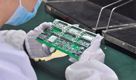
Visual PCB inspection serves as the initial, non-destructive step in PCB fault isolation, relying on human observation aided by magnification tools. Inspectors check for surface-level defects like scratches, burrs, solder bridges, missing components, and polarity errors under controlled lighting. This method proves essential for bare boards and assembled units, providing quick feedback on assembly quality. Standards such as IPC-A-600 define acceptability criteria for visual attributes, guiding engineers in consistent evaluations. While subjective, pairing it with checklists reduces variability and catches obvious issues before advanced testing.
Limitations arise with hidden defects or fine-pitch components, where naked eye resolution falls short. Engineers often combine visual checks with stereomicroscopes for detailed scrutiny of pad finishes and via fills. In production lines, this step feeds data into subsequent automated processes, streamlining PCB defect analysis. Regular training ensures inspectors align with class levels defined in relevant standards, maintaining factory precision.
Automated Optical Inspection (AOI): Speed and Precision for Surface Defects
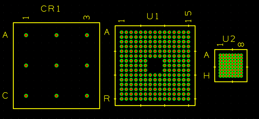
AOI represents an advancement in visual PCB inspection, employing high-resolution cameras and algorithms to scan boards post-solder paste printing, component placement, or reflow soldering. It detects anomalies such as insufficient solder, tombstoning, bridging, and misalignment by comparing actual images against golden samples or CAD data. This technique excels in high-volume surface-mount technology lines, offering rapid throughput without physical contact. Electric engineers value AOI for its repeatability, reducing human error in detecting defects down to micron levels.
Programming AOI systems requires defining defect thresholds based on assembly tolerances, ensuring false calls stay minimal. Multi-angle lighting enhances detection of lifted leads or shadows on ball grid arrays. Integration with manufacturing execution systems allows real-time PCB defect analysis and process adjustments. Despite strengths, AOI cannot inspect obscured areas like under components, necessitating complementary methods.
Automated X-ray Inspection (AXI): Revealing Hidden Faults
AXI employs X-ray imaging to penetrate solder joints and multi-layer structures, making it indispensable for PCB fault isolation in complex assemblies. X-ray inspection for hidden PCB defects enables manufacturers to detect internal anomalies that cannot be identified through surface-level inspection methods alone, especially in densely populated and multilayer PCB designs. It uncovers voids in BGA solder balls, barrel cracks in vias, and misalignment in blind vias that evade optical methods. Transmission or 3D tomographic modes provide volumetric data, aiding precise defect localization. Engineers select AXI for high-density interconnect boards where density obscures traditional views.
Oblique-angle views simulate cross-sections, facilitating quantitative analysis of joint fillet formation. Calibration to material densities ensures accurate interpretation across copper thicknesses. In production, AXI supports statistical process control by logging defect trends. While slower than AOI, its non-destructive nature justifies use in critical applications.
Electrical Testing: Flying Probe and In-Circuit Testing ICT
Flying probe testing uses movable probes to access test points, verifying continuity, shorts, resistance, and capacitance without custom fixtures. Ideal for low-to-medium volumes or prototypes, it adapts to diverse board layouts via software-defined nets. Probes make thousands of measurements per minute, isolating opens, wrong values, or polarity issues efficiently. Electric engineers appreciate its flexibility for double-sided boards and irregular geometries.
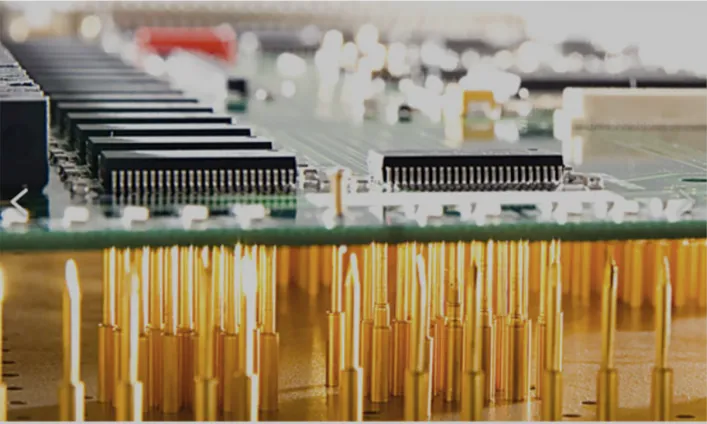
In contrast, in-circuit testing ICT deploys a bed-of-nails fixture for parallel probing, suiting high-volume runs with fixed test points. It performs parametric tests on components like resistors, capacitors, and diodes alongside boundary scans. ICT excels in detecting assembly faults early, before functional stages. Both methods align with J-STD-001 guidelines for electrical integrity post-assembly.
Guardrails prevent probe damage to fine-pitch parts, with vectorless modes enhancing fault coverage. Combining flying probe with ICT optimizes coverage across production scales.
Functional PCB Testing: System-Level Validation
Functional PCB testing evaluates the assembled board under operating conditions, simulating end-use scenarios to confirm overall performance. It applies power, inputs signals, and monitors outputs for logic, timing, and power integrity issues. Unlike component-focused tests, it reveals interactions like crosstalk or thermal effects missed earlier. Engineers script tests mimicking application profiles, including environmental stresses.
Boundary scan integration via JTAG enhances accessibility for embedded faults. This stage confirms no latent defects escaped prior isolations. Yield data informs root cause PCB defect analysis upstream.
Best Practices in PCB Defect Analysis and Fault Isolation
Integrate methods hierarchically: start with visual PCB inspection and AOI for gross defects, escalate to AXI and electrical tests for confirmation. Incorporating PCB fault isolation best practices into this workflow helps engineers narrow defect locations faster, reduce unnecessary rework, and improve diagnostic accuracy across both prototype and mass-production environments. Document findings in a centralized database for trend analysis, correlating defects to process parameters. Cross-train teams on standards like IPC-6012 to standardize classifications. Calibrate tools regularly and validate programs against known good boards.
For persistent issues, employ fishbone diagrams to trace root causes from materials to handling. Advanced PCB fault isolation best practices also recommend segmenting circuits into functional blocks, using boundary-scan testing and signal tracing to isolate intermittent or hidden electrical faults before component replacement. Simulate failures in design reviews to preempt common pitfalls. Prioritize high-risk areas like power planes and high-speed signals, where impedance inconsistencies, thermal stress, or solder integrity problems can rapidly propagate failures across the PCB assembly.
Troubleshooting Common PCB Faults
Engineers encounter opens from via drill misalignment, addressable via AXI slice views. Solder voids demand reflow profile tweaks, verified by functional margins. Component shifts require placement machine audits, caught early by AOI. Layer shorts benefit from flying probe isolation to pinpoint nodes.
Multidisciplinary reviews accelerate resolution, leveraging data from all tools.
Conclusion
PCB fault isolation evolves from visual PCB inspection to advanced AOI, AXI, flying probe testing, ICT, and functional PCB testing, forming a comprehensive quality shield. Electric engineers achieve optimal results by layering techniques aligned with IPC standards. Proactive PCB defect analysis drives continuous improvement in yields and reliability. Implementing these practices ensures robust electronics production.
FAQs
Q1: What distinguishes AOI from AXI in PCB fault isolation?
A1: AOI uses optical imaging for surface defects like misalignment and solder bridges, ideal for post-placement checks. AXI penetrates layers with X-rays to detect internal voids and via issues invisible to optics. Engineers choose AOI for speed in SMT lines and AXI for BGA-heavy boards. Combining both maximizes coverage in PCB defect analysis.
Q2: When should flying probe testing replace in-circuit testing ICT?
A2: Flying probe suits prototypes or low-volume runs due to no-fixture flexibility and adaptability to design changes. ICT thrives in high-volume with parallel probing for faster throughput on standardized boards. Both verify continuity and component values per J-STD-001. Select based on production scale for efficient PCB fault isolation.
Q3: How does functional PCB testing complement earlier methods?
A3: Functional testing validates system interactions after visual PCB inspection, AOI, and electrical tests catch isolated faults. It uncovers timing or power issues from component interplay. Engineers use it post-ICT to confirm end-performance. This holistic approach ensures reliability in complex assemblies.
Q4: What role do standards play in visual PCB inspection?
A4: Standards like IPC-A-600 provide criteria for acceptability of surface features, ensuring uniform defect calls. They classify boards by end-use, guiding inspector training. Consistent application reduces variability in factory PCB fault isolation workflows.
References
IPC-A-600K — Acceptability of Printed Boards. IPC, 2020
IPC-6012E — Qualification and Performance Specification for Rigid Printed Boards. IPC, 2017
J-STD-001J — Requirements for Soldered Electrical and Electronic Assemblies. IPC, 2020


