 00:54
00:54
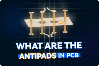
PCB Pad Design
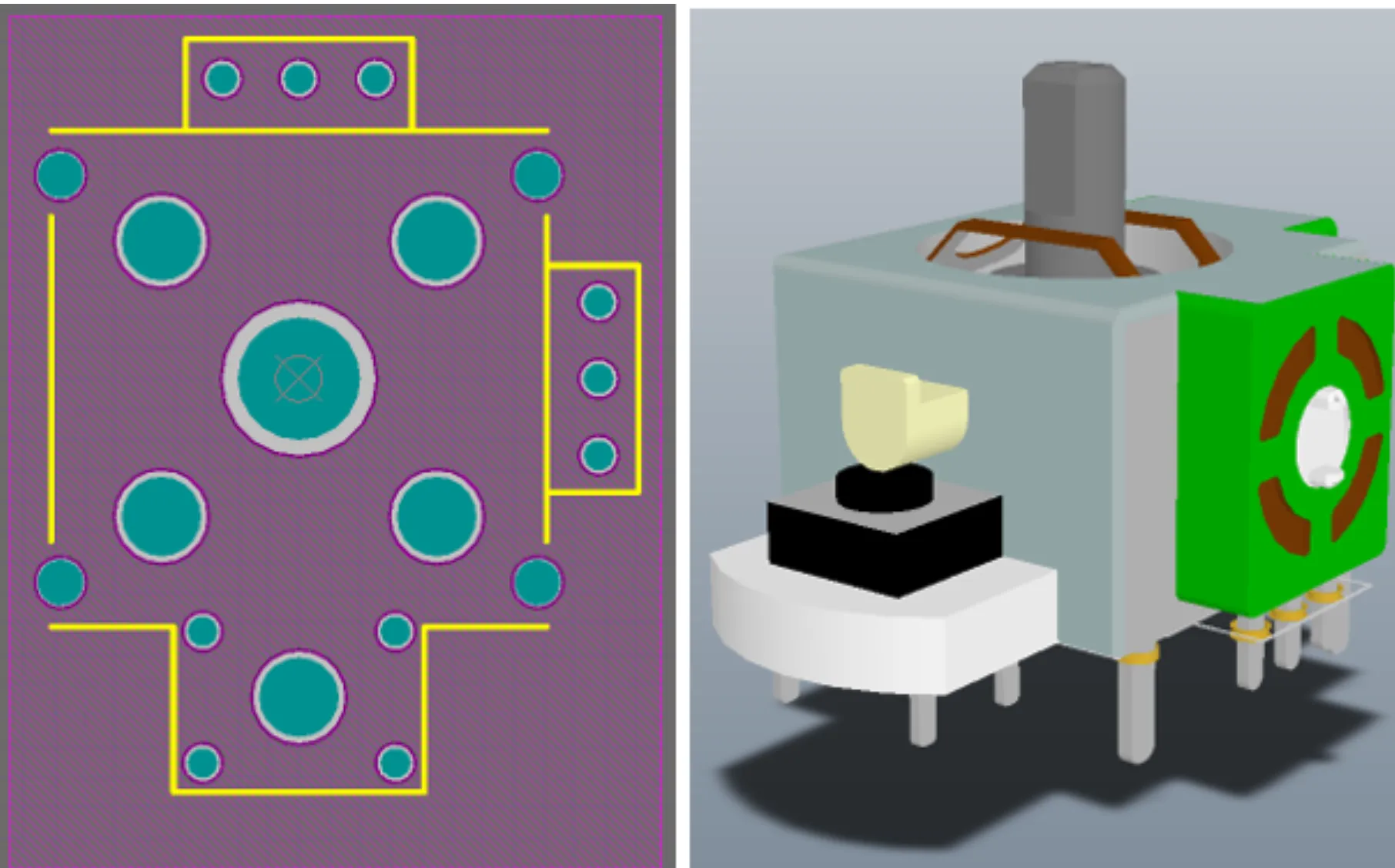
PCB pad design is a fundamental aspect of printed circuit board (PCB) engineering that directly impacts the reliability, manufacturability, and performance of electronic assemblies. Pads serve as the critical interface points where components are soldered onto the board, facilitating electrical connections and mechanical stability. For engineers and designers searching for PCB pad design resources, this tag compiles essential information on optimizing pad geometries, including shapes, sizes, and spacing to ensure robust solder joints and minimize defects such as tombstoning or bridging. Understanding these elements is vital for achieving high-yield production, especially in high-density layouts where signal integrity and thermal management become paramount. Effective PCB pad design incorporates best practices tailored to specific applications, such as adjusting pad dimensions for surface-mount devices (SMDs) to accommodate reflow soldering processes or incorporating thermal reliefs for through-hole components to prevent heat dissipation issues. Designers often face challenges like pad lift-off during assembly or impedance mismatches in high-speed circuits, which can be mitigated through careful consideration of materials, layer stackups, and industry standards like IPC-7351. By focusing on these actionable insights, users can enhance board durability and reduce rework costs. The articles under this tag provide in-depth discussions on these topics, offering practical guidelines for both novice and experienced practitioners to refine their designs and troubleshoot common problems. Whether you are prototyping a new circuit or scaling up for mass production, exploring the content here equips you with the knowledge to make informed decisions that align with manufacturing constraints and performance requirements. This ensures your PCBs not only meet functional specifications but also stand up to real-world environmental stresses, from vibration to temperature fluctuations.
Video Guide
-
00:54
Technical Articles
Get in Touch
Send Message
- Products & Service
- Company
- About AIVON
- Contact
- News
- Blog
- Certification
-


- Payment
-


2026 AIVON.COM All Rights Reserved