Introduction
In advanced PCB design, engineers often encounter non-standard components that do not fit predefined library footprints. These unique parts, ranging from custom sensors to specialized power modules, demand custom PCB footprints to ensure reliable assembly and performance. While standard footprints promote consistency across the industry, blindly adhering to them can lead to soldering defects or mechanical failures with irregular components. This article explores when to deviate from conventions through unique footprint design and provides structured guidance on footprint modification. By understanding the engineering rationale behind these decisions, electric engineers can balance innovation with manufacturability. Mastering custom footprints elevates complex component footprints from potential risks to optimized solutions.
What Are Custom Component Footprints and Why They Matter
A custom PCB footprint represents the precise arrangement of pads, vias, and mechanical outlines tailored to a specific non-standard component's dimensions and pin configuration. Unlike generic library entries, these footprints account for variations in lead pitch, body size, or thermal requirements that standard designs overlook. In high-reliability applications, such as aerospace or medical devices, mismatched footprints can compromise solder joint integrity, leading to intermittent failures under vibration or thermal cycling. Custom designs matter because they enable the integration of cutting-edge non-standard components, fostering advanced PCB design without sacrificing quality. Engineers must weigh the trade-offs: while standards streamline production, custom footprints allow for performance optimization in unique scenarios. Ultimately, they bridge the gap between component innovation and robust PCB assembly.
When to Create Custom PCB Footprints: Recognizing the Need to Break Rules
Standard footprints suffice for most common components, but custom PCB footprints become essential when datasheets reveal discrepancies from library norms. For instance, a non-standard component might feature an irregular lead toe or heel dimension that risks tombstoning during reflow if using off-the-shelf patterns. Engineers should create unique footprint designs for prototypes incorporating obsolete parts revived for legacy systems or bespoke modules from suppliers without published land patterns. Breaking rules is justified in high-density boards where space constraints demand footprint modification to improve routing density without violating clearance rules. However, avoid customs unless necessary, as they introduce verification overhead and potential assembly variability. The decision hinges on risk assessment: if standard footprints yield poor simulated solder fillet formation, customization prevents downstream issues.
Another trigger arises in thermal management scenarios, where non-standard components with exposed pads require enlarged thermal reliefs beyond generic specs. Vibration-prone environments also necessitate reinforced pad shapes, deviating from nominal guidelines to enhance mechanical anchorage. Procurement teams signal the need when sourcing unique components lacking JEDEC outlines, prompting in-house footprint development. By documenting the rationale, engineers ensure traceability, aligning custom choices with project requirements. This structured approach minimizes errors in complex component footprints.
Technical Principles Guiding Unique Footprint Design
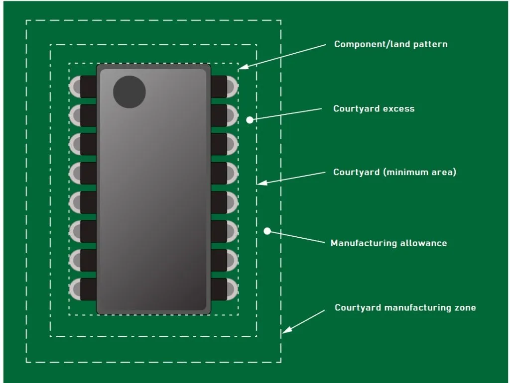
IPC-7351B outlines three density levels—most, nominal, and least—for land pattern geometry, providing a foundation even for custom PCB footprints. Engineers select density based on assembly process: least for high-volume reflow with tight tolerances, most for hand soldering where larger pads aid alignment. Pad width typically equals lead width plus toe overhang, while length accommodates heel fillet for reliable wetting. Courtyard excess ensures component spacing prevents solder bridging, calculated as body outline plus minimum keep-out zones. For through-hole variants, annular ring size follows similar scaling to maintain barrel fill during plating.
Solder joint mechanics drive footprint modification decisions. The toe, heel, and side fillet dimensions must promote uniform reflow, avoiding fillet lifting from CTE mismatch. Vias in complex component footprints require dog-bone routing or filled designs to handle current without thermal hotspots. Polarity indicators and fiducials enhance pick-and-place accuracy for non-standard components. Mechanical stability principles dictate silkscreen outlines slightly larger than body dimensions, aiding visual inspection post-assembly.
Thermal dissipation influences pad stackup, where exposed pads in QFN-like packages demand via arrays tented to control solder volume. Electrical performance considerations include trace escape routing from fine-pitch leads, ensuring impedance control in high-speed signals. These principles form a logical framework, transforming ad-hoc customs into engineered solutions.
Best Practices for Designing and Implementing Complex Component Footprints
Begin footprint creation with meticulous datasheet extraction: measure lead pitch, coplanarity, and body tolerances using calipers for prototypes. Cross-verify with 3D models if available, scaling pads accordingly. Employ IPC-7351B calculators conceptually—without software—to derive pad geometries, adjusting for process capabilities like stencil thickness. Prototype a test coupon with the custom PCB footprint to validate reflow profiles and inspect joints against J-STD-001 criteria for fillet height and wetting.
Document deviations explicitly: note density level chosen and rationale in library attributes for team review. Simulate solder paste deposition to predict bridging risks in dense arrays. For multilayer boards, align vias with inner plane cutouts to prevent stub effects. Iterate through design reviews, incorporating fab feedback on drill sizes and aspect ratios.
Collaborate early with assembly partners on footprint modification feasibility, focusing on feeder compatibility for non-standard components. Standardize naming conventions, like appending "_Custom_v1" to part numbers, for library management. Post-assembly, analyze X-ray or cross-sections to refine future designs, closing the feedback loop. These practices ensure custom footprints enhance rather than hinder advanced PCB design.
Case Study: Troubleshooting a Footprint Modification for High-Power Module
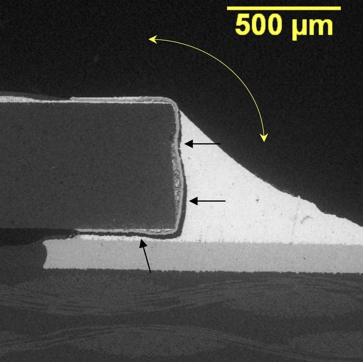
Consider a scenario where a non-standard power module's datasheet specified a 0.8 mm lead pitch but exhibited 10% coplanarity variation, causing open joints in initial prototypes. The engineering team opted for unique footprint design using nominal density per IPC-7351B, extending heel length by 20% to compensate. Initial reflow trials revealed insufficient toe fillet, prompting pad widening and stencil aperture reduction.
Further analysis via thermal imaging showed hotspots from poor via thermal relief, addressed by adding staggered vias under the pad. After three iterations, J-STD-001 compliant joints achieved 100% yield, with shear strength exceeding requirements. Key lesson: iterative validation prevents over-customization. This case underscores systematic troubleshooting for complex component footprints.
Conclusion
Creating custom PCB footprints demands disciplined engineering judgment to integrate non-standard components effectively. By recognizing when standards fall short and applying principles from IPC-7351B and J-STD-001, designers mitigate risks in advanced PCB design. Best practices like datasheet fidelity, density selection, and prototyping ensure reliable outcomes. Unique footprint design empowers innovation while upholding manufacturability. Electric engineers who master footprint modification gain a competitive edge in tackling complex challenges. Prioritize verification to turn potential pitfalls into strengths.
FAQs
Q1: When should electric engineers create a custom PCB footprint for non-standard components?
A1: Custom PCB footprints are warranted when datasheet dimensions deviate significantly from library standards, risking solder defects like tombstoning or bridging. Assess via simulation or test coupons, especially for prototypes or high-reliability apps. Follow IPC-7351B density guidelines to justify modifications logically. This approach balances performance with assembly yield.
Q2: How does IPC-7351B guide unique footprint design?
A2: IPC-7351B provides land pattern geometries across density levels, enabling engineers to scale pads for custom PCB footprints. Select least density for high-volume SMT, nominal for general use. It ensures optimal toe-heel fillets for reflow reliability. Apply these principles to non-standard components for consistent results.
Q3: What are common pitfalls in complex component footprints and how to avoid them?
A3: Overlooking coplanarity leads to open joints; mitigate by extending pad lengths per datasheet tolerances. Ignoring courtyard excess causes bridging—maintain 0.25 mm minimum. Prototype and inspect against J-STD-001 for wetting. Footprint modification succeeds through iteration and documentation.
Q4: Can footprint modification improve advanced PCB design outcomes?
A4: Yes, targeted changes like via arrays enhance thermal performance in unique footprint designs. Align with process capabilities to boost yield. For non-standard components, customization prevents failures in dense layouts. Logical application yields robust, high-performance boards.
References
IPC-7351B — Generic Requirements for Surface Mount Design and Land Pattern Standard. IPC, 2010
J-STD-001G — Requirements for Soldered Electrical and Electronic Assemblies. IPC, 2017


