Introduction
Ground loops represent a common challenge in PCB design that can compromise signal integrity and introduce unwanted noise. These loops form when multiple ground paths exist between circuit sections, allowing currents to flow in unintended directions and create voltage differentials. In high-density or mixed-signal boards, pcb ground loops exacerbate electromagnetic interference, or pcb design emi issues, leading to erratic performance or compliance failures. Engineers must address grounding techniques early in the schematic phase to ensure robust designs. Proper schematic grounding lays the foundation for reducing noise throughout the layout and fabrication process. By adopting structured approaches, designers can minimize these risks and achieve reliable operation.
This article explores the principles behind pcb ground loops, their causes, and proven grounding techniques for schematics. It provides practical best practices tailored for electric engineers working on complex boards. Understanding these concepts helps in creating designs that meet performance expectations without costly revisions. Schematic decisions directly influence layout success, making early intervention critical. With adherence to established guidelines, teams can enhance overall system stability.
What Are PCB Ground Loops and Why Do They Matter?
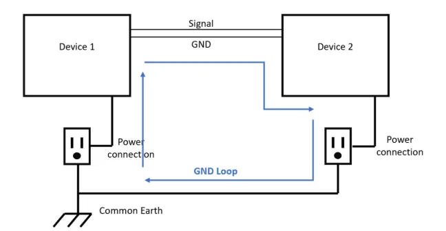
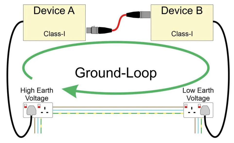
A pcb ground loop occurs when a circuit has more than one path to ground, forming a closed loop through which current can circulate. This current, often from external sources or internal imbalances, generates magnetic fields that induce voltage drops across the loop. In PCB schematics, these loops manifest as differing ground potentials between analog and digital sections, amplifying noise coupling. The result is degraded signal-to-noise ratios, particularly in sensitive applications like sensors or communications.
The relevance of avoiding pcb ground loops cannot be overstated in modern electronics. They contribute significantly to pcb design emi by radiating interference or picking up external noise. Compliance with electromagnetic compatibility requirements becomes challenging when loops persist into the layout stage. Reducing noise through effective schematic grounding ensures cleaner signals and better power distribution. Engineers prioritizing this from the start avoid prototyping delays and field failures.
In mixed-signal designs, ground loops couple high-frequency digital switching noise into low-level analog paths. This phenomenon distorts measurements and triggers false triggers in control systems. Industry practices emphasize unified ground references to maintain equipotential surfaces. By defining clear grounding strategies in schematics, designers set the stage for low-impedance return paths.
Causes of Ground Loops in PCB Schematics
Multiple ground symbols in schematics often lead to pcb ground loops during layout implementation. When analog and digital components connect to separate ground nets without intentional bridging, unintended paths form via power supplies or connectors. Poor planning results in voltage gradients that drive loop currents, especially under dynamic loads.
External connections, such as USB ports or shielding, introduce additional ground references that conflict with onboard grounds. Schematics lacking explicit single-point connections allow these paths to multiply. High-current sections, like power amplifiers, exacerbate the issue by injecting ripple into shared returns.
Improper power supply decoupling in schematics contributes indirectly by allowing noise to propagate through ground nodes. Designers sometimes overlook return current paths, assuming layout will resolve them. In reality, schematic ambiguities propagate errors, increasing pcb design emi susceptibility.
Component placement hints in schematics can also seed loops if grounds cluster incorrectly. For instance, separating noisy digital ICs from precision analog without defined isolation creates potential differentials. Early identification of these causes enables proactive schematic revisions.
Key Grounding Techniques for Schematics
Grounding techniques begin with selecting the appropriate topology based on frequency and circuit complexity. Single-point, or star, grounding connects all ground returns to one node, ideal for low-frequency designs below 1 MHz. This method eliminates loops by ensuring a common reference, though it demands careful node management in schematics.
For higher frequencies, multipoint grounding via a solid plane offers low inductance returns. Schematics should denote dedicated ground planes early, using net labels like "GND_PLANE" for clarity. This approach distributes return currents evenly, reducing noise voltage drops.
In mixed-signal boards, split grounding separates analog and digital domains while connecting them at one point. Schematics must explicitly show this junction, often near the ADC or interface IC, to prevent cross-talk. Adhering to IPC-2221 guidelines for printed board design reinforces these techniques by stressing uniform reference planes.
Guard traces or moats around sensitive nets provide additional shielding in schematics. These evolve into layout features but start as annotated boundaries. Combining techniques yields optimal results for reducing noise.
Best Practices for Schematic Grounding to Avoid Loops
Start schematic design with a unified ground symbol across the entire netlist. Assign all grounds to a single "GND" net unless splits are required, using hierarchical blocks for clarity. This practice streamlines net assignment and flags potential multi-path issues during review.
Explicitly define power entry points and their ground returns in the schematic. Place decoupling capacitors close to IC pins with direct ground connections, minimizing local loops. Net classes for analog and digital grounds help enforce separation.
Incorporate shielding notes for high-speed signals, routing them with adjacent ground references. Use bus structures for multi-ground signals from connectors, converging to the main ground node. These steps align with schematic grounding principles that reduce noise propagation.
For multilayer boards, pre-allocate ground plane layers in stackup notes within the schematic documentation. Simulate ground impedance early using tools to validate topologies. Regular DRC checks catch duplicate ground symbols before export.
Document grounding rationale in schematic sheets, including frequency considerations for single versus multipoint. Collaborate with layout teams by exporting annotated PDFs highlighting critical nets. This ensures translation fidelity.
Transitioning from Schematic to Layout for EMI Control
Schematic grounding sets constraints that layout must honor to combat pcb design emi. Export netlists with ground plane directives, specifying pour orders and stitching vias. Layout engineers flood planes first, verifying no splits disrupt returns.
Place components to minimize trace lengths from pins to ground vias. Under mixed-signal ICs, partition planes but bridge with narrow traces or 0-ohm resistors at designated points. This maintains schematic intent while providing flexibility.
Via stitching along board edges and partitions secures plane integrity. For chassis grounds, schematics should note isolated connections via capacitors to break DC loops. Post-layout simulations confirm impedance targets.
Following IEC standards for electromagnetic compatibility supports these transitions by emphasizing low-impedance grounds. Thorough reviews bridge schematic and layout phases effectively.
Troubleshooting Common Ground Loop Issues
Suspect pcb ground loops when noise spectra show 50/60 Hz hum or switching harmonics on scopes. Probe ground nodes across the board to map voltage differentials exceeding millivolts. Correlate with schematic nets to identify multi-path culprits.
In prototypes, isolate sections by lifting ground pins and measuring improvements. Spectral analysis reveals loop-induced spurs. Adjust by consolidating grounds per schematic best practices.
Simulation tools replay schematic currents on layout models, pinpointing high-loop areas. Iterate with ferrite beads or RC filters on suspect returns. Persistent issues often trace to unconnected chassis grounds.
Field failures post-assembly demand schematic audits for overlooked connector grounds. Firmware tweaks rarely suffice; hardware revisions focus on grounding fixes.
Conclusion
Mastering schematic grounding eliminates pcb ground loops, ensuring low-noise, EMI-compliant designs. Key techniques like single-point and plane-based grounding, applied logically from the start, yield robust results. Best practices emphasize unified nets, explicit splits, and documentation for seamless layout handoff. Electric engineers benefit from structured approaches that align with industry standards. Prioritizing these steps reduces risks and accelerates development. Implement them consistently for superior PCB performance.
FAQs
Q1: What are the main grounding techniques to prevent pcb ground loops in schematics?
A1: Single-point star grounding connects all returns to one node, suitable for low frequencies, while multipoint uses planes for high-speed signals. Split planes for mixed-signals require single-point bridging to avoid differentials. Annotate schematics clearly to guide layout. These methods reduce noise by providing low-impedance paths.
Q2: How does schematic grounding impact pcb design emi?
A2: Poor schematic grounding creates loops that radiate interference or couple noise, failing EMC tests. Unified ground nets minimize return path inductance, curbing emissions. Early planning ensures layout compliance. Engineers see measurable EMI drops with solid planes.
Q3: When should you use split ground planes in PCB schematics?
A3: Use splits in mixed-signal designs to isolate analog from digital noise, connecting at one point near converters. Avoid arbitrary splits that form loops. Schematic notes specify stitching locations. This balances isolation and unity.
Q4: What role does IPC-2221 play in grounding techniques?
A4: IPC-2221 provides guidelines for PCB design, including reference planes and power distribution to minimize noise. It stresses uniform grounds for integrity. Designers reference it for schematic planning. Compliance aids reliability.
References
IPC-2221F — Generic Standard on Printed Board Design. IPC, 2022
IEC 61000-5-2 — Electromagnetic compatibility (EMC) — Part 5-2: Installation and mitigation guidelines — Screening, filtering and surge suppressors. IEC, 2020
J-STD-001H — Requirements for Soldered Electrical and Electronic Assemblies. IPC, 2021


