Introduction
In the competitive landscape of electronics design, PCB trace routing plays a pivotal role in balancing performance requirements with production economics. Engineers often face the challenge of creating functional circuits while keeping PCB manufacturing costs in check. Inefficient routing can lead to unnecessary increases in layer count, via density, and fabrication tolerances, all of which drive up expenses. By adopting targeted PCB trace routing optimization techniques, designers can achieve reliable signal integrity without inflating the PCB trace routing cost. This article explores proven strategies grounded in industry practices to help electric engineers minimize manufacturing overheads. Understanding these approaches ensures designs that are both robust and economical.
Understanding PCB Trace Routing and Its Impact on Manufacturing Costs
PCB trace routing refers to the process of defining conductive paths on a printed circuit board to interconnect components, carrying signals, power, and ground. These traces form the backbone of the board's electrical functionality, influencing everything from signal speed to thermal dissipation. Routing decisions directly affect PCB manufacturing cost through factors like material usage, processing steps, and yield rates. For instance, complex routing patterns may necessitate additional layers or specialized etching processes, escalating expenses. Compliance with standards such as IPC-2221 for conductor sizing helps maintain manufacturability. Ultimately, thoughtful routing reduces waste and aligns with fabrication capabilities for cost efficiency.
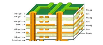
The relevance of PCB trace routing cost optimization stems from the multilayer nature of modern boards. Each additional layer introduces lamination cycles, alignment challenges, and higher material consumption, significantly impacting the bottom line. Vias, essential for interlayer connections, add drilling and plating costs, especially for blind or buried types. Poor routing can also lower yields due to defects like shorts or opens, leading to rework. Electric engineers must prioritize routing that maximizes board real estate while adhering to standard tolerances. This not only cuts PCB cost but also shortens lead times.
Key Principles of Cost-Effective PCB Trace Routing
Effective trace routing begins with fundamental electrical and mechanical principles that govern conductor performance. Trace width must support current-carrying capacity without excessive heating, as outlined in IPC-2221 guidelines for external and internal conductors. Spacing between traces prevents crosstalk and arcing, particularly in high-density designs. Engineers calculate these parameters based on voltage levels, dielectric properties, and environmental factors to avoid over-specification. Vias introduce impedance discontinuities, so minimizing their number preserves signal quality and reduces fabrication complexity. Layer stackup symmetry aids in controlling warpage during thermal cycling, indirectly supporting cost control.
Another core principle involves etch factor and manufacturing tolerances. During chemical etching, traces can undercut, narrowing widths and risking reliability. IPC-6012E specifies minimum conductor widths post-etching to ensure performance, guiding designers toward conservative geometries. Routing on outer layers is cheaper than inner ones due to simpler access for inspection and rework. Power and ground planes should integrate seamlessly with traces to shorten return paths and reduce inductance. These principles form the foundation for PCB trace routing optimization, enabling designs that scale economically.
Adhering to grid-based routing enhances alignment and repeatability. Using a consistent grid for component placement and trace bends facilitates automated fabrication. Sharp 90-degree corners create reflections in high-speed signals, so 45-degree miters or curves are preferable, though they must balance with space constraints. Thermal management influences routing, as wide traces dissipate heat better but consume more copper. By internalizing these mechanisms, engineers can preempt cost drivers early in the design phase.
Strategies for PCB Trace Routing Optimization
One primary strategy for lowering PCB trace routing cost is minimizing the number of layers through intelligent fanout and component placement. Group related signals on the same layer to reduce interlayer jumps, prioritizing power and ground on dedicated planes. This approach cuts lamination steps and material layers, directly impacting PCB manufacturing cost. For example, routing high-current paths on thicker outer foils avoids the need for paralleled inner traces. Pre-planning stackups with even copper distribution prevents registration issues during drilling.
Standardizing trace widths and spacings to common fabrication capabilities is another key tactic. Opt for geometries like 0.15 mm traces and spaces where possible, as finer features demand advanced photolithography and etching, raising costs. IPC-2221 provides charts for sizing based on current and temperature rise, allowing engineers to select manufacturable options. Avoid custom tolerances unless critical, as they trigger non-standard tooling. This uniformity boosts yield and enables volume pricing discounts.
Reducing via count through optimized paths significantly trims expenses. Through-hole vias are cheapest, so maximize surface routing before going multilayer. Employ stitching vias sparingly for plane connections and group them to share drill hits. Blind and buried vias, while space-saving, require sequential lamination, doubling costs. Daisy-chaining non-critical nets minimizes transitions. Post-layout analysis tools can identify via hotspots for redesign.
Efficient panel utilization via routing symmetry and border clearances enhances economies of scale. Design boards with v-scoring or tab-routing in mind, keeping traces away from edges to avoid delamination. Matched trace lengths for differential pairs can share layers, but prioritize cost over marginal skew corrections. Fanout patterns for BGA components should use dog-bone or via-in-pad judiciously, as the latter increases soldermask complexity.
Incorporating design for manufacturability (DFM) rules during routing prevents downstream issues. Route away from flex areas in rigid-flex boards and ensure clearance for fiducials. Power distribution networks should use wide buses to cut IR drop without extra layers. Iterative DRC checks catch violations early. These practices collectively drive down PCB trace routing cost without compromising integrity.
Common Pitfalls and Troubleshooting in Trace Routing
Engineers frequently encounter routing congestion leading to forced layer adds. Troubleshooting involves hierarchical routing: critical nets first, followed by clocks, then others. Overuse of jumpers or 0-ohm resistors as workarounds inflates assembly costs. Signal integrity simulations reveal crosstalk hotspots for rerouting. Warpage from asymmetric copper, exacerbated by poor trace balance, fails IPC-A-600 acceptability criteria. Redistributing copper density resolves this without added layers.
In high-density interconnects, via farms under components spike drill counts. Alternatives like embedded traces in thicker dielectrics trade cost for density. Yield killers like bridging arise from inadequate spacing; widening to standard rules mitigates this. Post-etch inspection data informs future optimizations. Addressing these pitfalls ensures robust, low-cost designs.
Conclusion
Cost-effective PCB trace routing demands a holistic approach integrating electrical principles, standards compliance, and fabrication realities. By minimizing layers, standardizing geometries, and curbing vias, engineers can substantially reduce PCB manufacturing cost. Strategies like grid alignment and DFM integration yield reliable boards at scale. Adopting these techniques not only optimizes PCB trace routing cost but elevates overall design efficiency. Electric engineers equipped with this knowledge deliver value-driven solutions in demanding projects.
FAQs
Q1: How does PCB trace routing optimization impact overall manufacturing costs?
A1: PCB trace routing optimization lowers costs by reducing layer counts, via usage, and custom tolerances, aligning with standard fabrication processes. Fewer layers mean less material and lamination cycles, while standard trace widths boost yields. Compliance with IPC-2221 ensures manufacturable designs without premium pricing. This holistic approach can cut PCB manufacturing cost by streamlining production flows for electric engineers.
Q2: What are the main strategies to minimize PCB trace routing cost?
A2: Key strategies include standardizing trace spacings, minimizing vias through efficient surface routing, and optimizing layer stackups for symmetry. Route power planes first to free signal layers, and use grid-based paths for alignment. Avoid blind vias unless essential, as they inflate drilling expenses. These tactics directly target PCB trace routing cost while maintaining signal integrity per industry guidelines.
Q3: Why is via reduction critical for PCB manufacturing cost control?
A3: Vias add drilling, plating, and inspection steps, with each type carrying distinct costs: through-hole cheapest, buried most expensive. Reducing vias via smart component placement and single-layer fanout cuts these operations. Grouped vias share hits, further saving. In PCB trace routing optimization, this preserves budget without sacrificing connectivity for multilayer boards.
Q4: How do standards like IPC-2221 influence cost-effective trace routing?
A4: IPC-2221 provides sizing charts for traces based on current and voltage, guiding engineers to practical widths that avoid overdesign. It promotes spacings that prevent defects, enhancing yields and lowering rework. By following these, designs fit standard fab capabilities, reducing PCB trace routing cost. Electric engineers leverage it for balanced performance and economy.
References
IPC-2221B — Generic Standard on Printed Board Design. IPC, 2012
IPC-6012E — Qualification and Performance Specification for Rigid Printed Boards. IPC, 2017
IPC-A-600K — Acceptability of Printed Boards. IPC, 2020


