Introduction
Differential pair routing forms a core part of modern PCB layout for beginners venturing into high-speed designs. Electronic hobbyists often encounter these pairs when working on projects involving USB connections, Ethernet interfaces, or display signals. Proper routing ensures clean signal transmission without distortion or noise interference. This guide covers differential pair routing basics, making PCB layout for beginners accessible and practical. You will learn signal integrity tutorial essentials, including impedance matching explained in simple terms. By following these steps, you can achieve easy PCB design results that perform reliably in your hobby circuits.
Many hobbyists start with single-ended signals but quickly realize the need for differential pairs as speeds increase. These pairs reject common-mode noise effectively, preserving data integrity. Understanding the fundamentals helps avoid common pitfalls like crosstalk or skew. This article provides a structured path from theory to hands-on routing. Whether prototyping a sensor board or a communication module, mastering these techniques elevates your projects.
What Are Differential Pairs?
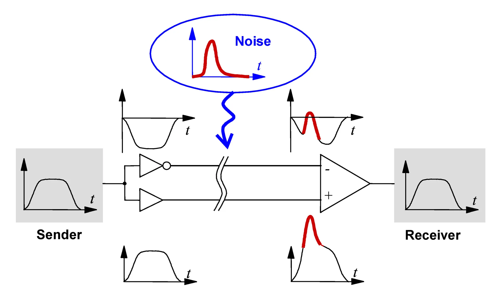
A differential pair consists of two closely spaced traces that carry equal but opposite signals relative to each other. The receiver detects the difference between these signals, canceling out external noise picked up equally by both traces. This setup is ideal for high-speed data transmission in hobby projects. Common examples include USB 2.0 pairs at 480 Mbps or LVDS for LCD panels. In PCB design, these pairs maintain balance to preserve signal quality over distance.
The positive trace carries the original signal, while the negative trace inverts it. Noise coupling into both traces appears as common-mode and gets rejected at the differential receiver. This principle underpins signal integrity in many interfaces. Hobbyists benefit from this noise immunity in noisy environments like motor control boards. Defining pairs early in the schematic ensures smooth transition to layout.
Why Differential Pair Routing Matters
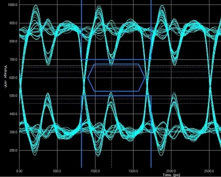
Signal integrity tutorial highlights how poor routing leads to bit errors, eye diagram closure, or electromagnetic interference. In PCB layout for beginners, ignoring differential pairs can cause project failures at higher frequencies. Proper routing minimizes reflections, crosstalk, and timing skew. For electronic hobbyists, this means reliable operation without expensive oscilloscopes for debugging. Impedance mismatches amplify these issues, distorting waveforms.
Industry relevance grows with faster hobby microcontrollers and peripherals. Standards like IPC-2221 emphasize uniform conductor geometries for controlled performance. Differential routing reduces radiated emissions, aiding FCC compliance for personal projects. It also lowers susceptibility to nearby power lines or motors. Mastering these basics unlocks advanced designs like Gigabit Ethernet adapters.
Key Principles of Differential Pair Routing Basics
Start with impedance matching explained: each pair must present a consistent differential impedance, typically 90 to 120 ohms depending on the standard. This value arises from trace width, spacing, thickness, and dielectric height. The two traces couple tightly, forming a transmission line. Deviations cause reflections that degrade signals. Calculate using stackup parameters for accuracy.
Length matching keeps propagation delays equal, preventing skew. Aim for tolerances under 5 mils for multi-GHz signals, looser for slower hobby uses. Constant edge-to-edge spacing preserves coupling and impedance. Route pairs parallel on the same layer to avoid mode conversion. Reference planes beneath provide return paths, reducing loop inductance.
Avoid 90-degree bends; use 45-degree or curved turns. Symmetry in vias and meanders maintains balance. IPC-2221 guidelines support these practices through spacing and width rules. Ground stitching vias near turns shield against crosstalk.
Step-by-Step Guide to Easy PCB Design with Differential Pairs
Step 1: Define Pairs in Your Design Environment
Assign nets as differential pairs during schematic capture. Label them like USB_DP and USB_DN. This enables automatic rule application in layout. Set differential impedance target, say 90 ohms for USB. Verify connectivity before routing.
Step 2: Configure Routing Rules
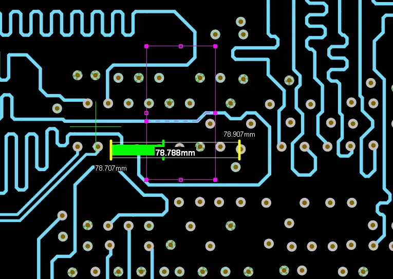
Specify trace width, gap between traces, and length mismatch tolerance. For FR4 material at 1.6 mm thickness, widths around 6 mils and gaps 8 mils suit 100-ohm pairs. Enable length tuning for matching. Minimum clearance to other nets prevents coupling.
Step 3: Select Optimal Layer and Reference Plane
Route on inner layers for better shielding if multilayer. Ensure solid ground plane below and above. Avoid splits under pairs; use power planes cautiously. Hobbyists often use 2-4 layer boards effectively.
Step 4: Route the Pair Parallel and Symmetrically
Draw traces side-by-side with constant spacing. Fanout from pins symmetrically. Use interactive routing modes for diff pairs. Maintain minimum bend radius.
Step 5: Implement Length Matching
Use serpentine meanders on the longer trace. Place tuning near the end to minimize impact. Verify total lengths match within tolerance. Simulate if possible for high speeds.
Step 6: Handle Vias and Transitions
Place vias in pairs, same location relative to traces. Back-drill if needed for stubs. Transition layers symmetrically.
Step 7: Verify and Optimize
Run design rule checks for spacing, length, and impedance. Visually inspect for symmetry. Export stackup for external impedance verification.
Best Practices for Signal Integrity Tutorial
Tight coupling reduces common-mode noise conversion. Keep intra-pair gap 4-6 times trace width for edge-coupled pairs. Broader spacing suits loose coupling. Solid reference planes cut inductance. Stitch vias every lambda/20 along routes.
Minimize vias; use blind or buried where possible. Route away from clocks or power. IPC-2141 provides methods for controlled impedance verification. For hobbyists, these steps ensure gigabit speeds without issues.
Guard traces or ground fills between pairs block crosstalk. Control layer transitions carefully.
Common Mistakes and Troubleshooting in PCB Layout for Beginners
Unequal lengths cause skew, flipping eyes closed. Solution: always tune post-routing. Variable spacing alters impedance; measure consistently. Routing over plane splits converts modes; bridge splits.
Placing aggressive signals between pairs induces crosstalk. Vias too far apart unbalance pairs. Beginners forget symmetry in bends. Troubleshoot with TDR if available, or scope differentials.
Conclusion
Differential pair routing basics empower electronic hobbyists to tackle signal integrity tutorial challenges confidently. From impedance matching explained to length tuning, these steps form easy PCB design foundations. Follow the guide for reliable high-speed interfaces in your projects. Consistent practices aligned with standards yield professional results. Experiment iteratively, starting simple.
FAQs
Q1: What are the differential pair routing basics for hobbyists?
A1: Differential pair routing basics involve two parallel traces with equal lengths, constant spacing, and matched impedance for noise rejection. Set rules for width around 5-10 mils and gaps 6-12 mils on standard stackups. Route on the same layer over ground planes. Length match within 10 mils for speeds under 1 Gbps. This ensures signal integrity tutorial success in USB or Ethernet hobby projects.
Q2: How does impedance matching explained work in PCB layout for beginners?
A2: Impedance matching explained means designing traces to a target like 100 ohms differential by controlling width, spacing, and dielectric. Use formulas or calculators based on stackup. Consistent geometry prevents reflections. Verify with field solvers if advanced. Beginners focus on rules during routing for easy PCB design. Poor matching distorts signals at transitions.
Q3: What role does length matching play in signal integrity tutorial?
A3: Length matching in signal integrity tutorial equalizes delays between pair traces, minimizing skew. Use serpentine patterns on longer traces. Tolerances of 5-20 mils suit most hobby speeds. Verify post-layout. Mismatch causes timing errors in data eyes. Essential for multi-gigabit interfaces.
Q4: Why avoid plane splits under differential pairs in easy PCB design?
A4: Plane splits under differential pairs in easy PCB design disrupt return currents, increasing inductance and emissions. Route over solid ground. Bridge splits if unavoidable with stitching vias. This maintains low noise and integrity. Common beginner error in multilayer boards.
References
IPC-2221B — Generic Standard on Printed Board Design. IPC, 2003
IPC-2141 — Design Guide for High-Speed Controlled Impedance Circuit Boards. IPC, 1996
IPC-A-600K — Acceptability of Printed Boards. IPC, 2020


