Introduction
In modern PCB design, effective trace routing stands as a cornerstone for ensuring signal integrity, particularly in high-speed applications. PCB trace routing crosstalk emerges as a primary challenge, where unintended signal coupling between adjacent conductors degrades performance. Similarly, PCB trace noise reduction requires careful strategies to mitigate electromagnetic interference. Engineers must master these techniques to prevent issues like bit errors, timing skew, and system instability. This article explores proven methods grounded in engineering principles, focusing on PCB trace spacing and routing practices that optimize reliability. By applying these approaches, designers can achieve robust boards compliant with industry expectations.
Understanding Crosstalk and Noise in PCB Trace Routing
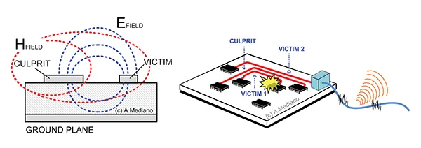
Crosstalk refers to the unwanted transfer of signals between traces due to electromagnetic coupling. In PCB trace routing, this occurs primarily through capacitive and inductive mechanisms. Capacitive crosstalk arises from electric fields between closely spaced traces, inducing voltage noise on a victim trace from an aggressor trace's switching. Inductive crosstalk stems from magnetic fields generated by current changes in the aggressor, linking to the victim via mutual inductance. Noise, often encompassing crosstalk alongside other interference, amplifies these effects, leading to signal distortion in sensitive circuits. Why does this matter? In high-frequency designs, even minor crosstalk can exceed noise margins, causing failures in data transmission or analog precision.
The relevance intensifies with rising clock speeds and denser boards. Electric engineers encounter these issues in RF, DDR memory, and SerDes interfaces. Poor management results in electromagnetic compatibility failures during compliance testing. Conversely, optimized routing enhances yield and reduces iterations. Addressing PCB trace routing crosstalk early preserves margins for other design variables like impedance control. Ultimately, mastering these fundamentals separates reliable prototypes from production-ready boards.
Technical Principles Behind Crosstalk and Noise
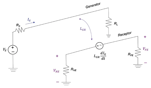
Crosstalk magnitude depends on coupling coefficients, which scale inversely with trace separation. For capacitive coupling, the coupling capacitance C_c is proportional to overlap length and dielectric permittivity, while inversely proportional to spacing. Inductive coupling L_m follows similar geometry dependence, peaking with parallel runs over shared reference planes. Noise sources compound this, including simultaneous switching on multiple aggressors or ground bounce from return path inductance. Engineers quantify these via field solver simulations or empirical formulas, revealing exponential decay in coupling strength with increased distance. Parallel trace length directly amplifies integrated crosstalk voltage, making minimization critical.
Key factors include rise time of signals and frequency content. Fast edges concentrate energy in higher harmonics, enhancing coupling efficiency. Without proper reference planes, fields extend further, worsening broadband noise pickup. Dielectric properties influence both mechanisms, with lower permittivity reducing capacitive coupling. Trace geometry, such as width and height above plane, modulates field confinement. Understanding these principles guides intuitive routing decisions before detailed analysis.
Standards like IPC-2221 provide foundational guidelines for conductor spacing to limit electric field effects, though high-speed designs demand extensions beyond voltage-based rules. These principles underscore that PCB trace spacing serves as the first line of defense against unintended interactions.
Best Practices for PCB Trace Spacing and Crosstalk Mitigation
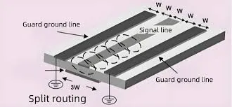
Optimal PCB trace spacing follows rules of thumb like the 3W guideline, where spacing equals three times the trace width to attenuate coupling significantly. This approach confines fields, reducing far-end crosstalk by orders of magnitude compared to minimal clearances. For critical nets, aim for 5W or more where density allows. Manufacturing capabilities dictate minimums, typically 4-6 mils, but signal integrity overrides for high-speed lines. Vary spacing dynamically: tighter for low-speed, generous for clocks and data buses. Verify via post-layout extraction to confirm compliance.
Minimize parallel run lengths between sensitive traces. Stagger alignments or use orthogonal routing on adjacent layers to break coupling paths. Limit victim-aggressor parallelism to under 1/10 of rise time propagation distance. Route high-speed signals between ground planes, leveraging microstrip or stripline configurations for field containment. Solid reference planes return currents locally, suppressing inductive loops that amplify noise.
Incorporate guard traces grounded at multiple points to shield victims. These act as Faraday cages, shunting coupled energy to ground before reaching the victim. Stitch guards to planes with vias every few wavelengths. For differential pairs, maintain tight coupling within the pair while isolating from singles. This common-mode rejection inherently combats PCB trace noise reduction challenges.
Advanced Techniques for PCB Trace Noise Reduction
Layer stacking plays a pivotal role in noise isolation. Dedicate inner layers to ground and power planes adjacent to signal layers. This sandwiches signals, minimizing radiation and coupling to outer layers. Avoid routing over plane splits, as they force lengthy return paths, inducing impedance discontinuities and noise. Use blind or buried vias to preserve plane integrity.
Impedance control complements spacing by matching trace characteristics to drivers and receivers. Consistent width and plane proximity yield 50-ohm singles or 100-ohm differentials, reducing reflections that masquerade as noise. Terminate lines appropriately to dampen ringing. For mixed-signal boards, segregate analog and digital partitions with ground moats or split planes tied at single points.
Simulation precedes fabrication: pre-layout stackup analysis predicts coupling budgets. Post-layout S-parameter extraction validates margins. Iterate routing to balance density and integrity. These techniques, aligned with IPC-6012 performance specs, ensure boards withstand real-world stressors.
Troubleshooting Common Routing Pitfalls
Engineers often overlook via fences near connectors, where dense transitions couple aggressively. Deploy arrays of grounded vias to form shields. Long meanders for length matching invite noise pickup; opt for serpentine with wide bends and ground proximity. Power traces parallel to signals induce ripple; separate or shield them.
In troubleshooting, scope victim nets during worst-case switching. Eye diagrams reveal crosstalk-induced jitter. Adjust spacing iteratively, prioritizing clocks last in routing order. These insights stem from systematic verification, preventing escapes to assembly.
Conclusion
Mastering PCB trace routing crosstalk demands a blend of spacing discipline, plane utilization, and geometric awareness. PCB trace noise reduction follows from confining fields and minimizing interactions. PCB trace spacing emerges as the simplest yet most effective lever, amplified by guards and references. Adhering to principles like those in IPC-2221 equips engineers for denser, faster designs. Implement these techniques methodically to elevate signal integrity. Future boards will demand even finer control, rewarding proactive expertise.
FAQs
Q1: What is the role of PCB trace spacing in reducing crosstalk?
A1: PCB trace spacing directly diminishes capacitive and inductive coupling by increasing distance between conductors. A common guideline suggests spacing at least three times the trace width for high-speed signals, confining electric and magnetic fields. This practice lowers induced noise voltage exponentially with separation. Combined with short parallel runs, it forms a robust first defense in PCB trace routing crosstalk mitigation. Engineers should tailor spacings to frequency and density constraints for optimal results.
Q2: How do ground planes contribute to PCB trace noise reduction?
A2: Ground planes provide low-inductance return paths, tightening current loops and reducing radiated emissions. Positioning signal traces close to planes confines fields, minimizing coupling to adjacent lines. Solid pours without splits prevent ground bounce that amplifies noise. Stitching vias enhance plane effectiveness at high frequencies. This strategy integral to PCB trace noise reduction supports compliance in multilayer boards.
Q3: What techniques minimize parallel trace coupling in routing?
A3: Limit parallel run lengths to less than one-tenth the signal rise time propagation. Stagger traces orthogonally across layers to break field overlap. Employ guard traces grounded frequently to absorb coupled energy. Differential routing with tight pair spacing rejects common-mode noise. These methods effectively combat PCB trace routing crosstalk in dense layouts.
Q4: Why follow IPC standards in trace routing?
A4: IPC standards like IPC-2221 offer proven spacing and layout guidelines ensuring reliability across voltages and environments. They guide conductor dimensions to limit arcing and coupling risks. Compliance facilitates manufacturing consistency and testing success. For high-speed, they provide baselines extended by signal integrity rules. This foundation aids PCB trace spacing decisions systematically.
References
IPC-2221B — Generic Standard on Printed Board Design. IPC, 2012
IPC-6012E — Qualification and Performance Specification for Rigid Printed Boards. IPC, 2017
J-STD-001H — Requirements for Soldered Electrical and Electronic Assemblies. IPC, 2020


