Introduction
Flex PCB impedance control plays a critical role in modern electronics where high-speed signals must travel through dynamically bending circuits. Flexible printed circuits, or flex PCBs, enable compact designs in applications such as wearables, medical devices, and aerospace systems. However, achieving consistent characteristic impedance in these structures presents unique hurdles due to material properties and mechanical stresses. This article explores the core principles behind impedance control flexible circuits, outlines key design challenges in flex PCB impedance, and delivers practical solutions for electrical engineers tackling flexible PCB design. By addressing these elements, designers can ensure signal integrity and reliability. Understanding these aspects aligns with industry needs for high-performance interconnects.
What Is Impedance Control in Flex Circuits and Why It Matters
Impedance control in flex circuits refers to the precise engineering of transmission line characteristics to maintain a target characteristic impedance, typically denoted as Z0, across the flexible substrate. In flexible PCBs, this involves configuring traces as microstrip or stripline configurations using polyimide films and copper conductors. The goal is to match the source and load impedances, minimizing reflections that degrade signal quality. For high-frequency signals, uncontrolled impedance leads to waveform distortion, increased bit error rates, and electromagnetic interference. In applications like data interfaces or RF modules, flex PCB impedance control becomes essential for preserving data rates and reducing power loss. Engineers must prioritize this from the initial design phase to meet performance specs in compact, movable assemblies.
The relevance of impedance control flexible circuits extends to industries demanding reliability under motion. Flexible PCB design without proper impedance management risks crosstalk between adjacent traces and attenuation over length. Standards like IPC-6013E outline qualification requirements that indirectly support impedance stability through material and construction specs. As signal speeds exceed gigabit rates, even minor deviations amplify issues, making precise control non-negotiable. Procurement teams and fabricators collaborate closely to verify tolerances, often targeting 10 percent variation. Ultimately, effective impedance control enhances overall system yield and longevity.
Technical Principles of Impedance in Flexible PCBs
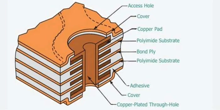
Characteristic impedance in flex circuits derives from the interaction of inductance per unit length and capacitance per unit length, governed by Z0 equals square root of L over C. Key factors include trace width, copper thickness, dielectric height, and the effective dielectric constant of materials like polyimide cores and coverlays. In microstrip designs common to single-layer flex, the signal trace sits atop the dielectric with air above, leading to a hybrid effective epsilon. Stripline configurations embed traces between ground planes, offering better shielding but requiring symmetric dielectrics. Manufacturing processes introduce variables such as adhesive flow and lamination pressure, which alter these dimensions. Engineers model these using field solver equations adapted for flexible substrates.
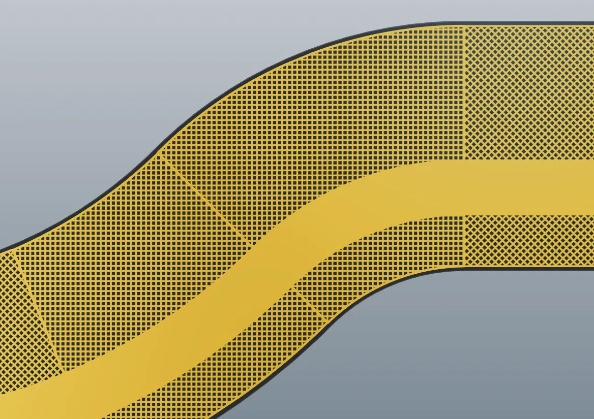
Hatched ground planes frequently appear in flex PCB impedance control to mitigate mechanical stress during bending, yet they modify field distribution and thus Z0. The hatch fill percentage influences return path effectiveness, with denser fills approximating solid planes but risking cracks. Polyimide's low dielectric constant aids higher impedances, but anisotropy under flex can shift values. Temperature and humidity further impact epsilon_r, demanding robust stackup choices. Dynamic bending compresses or expands dielectric height, dynamically altering capacitance. These principles underscore the need for iterative simulation in flexible PCB design.
Design Challenges in Flex PCB Impedance Control
One primary challenge in flex PCB impedance control stems from material inconsistencies, where dielectric thickness variations exceed those in rigid boards due to thinner films. Polyimide cores tolerate less deviation, amplifying sensitivity to etch tolerances in trace widths. Mechanical flexing introduces geometry changes, as repeated bends alter trace-to-plane spacing and induce microcracks in copper. This dynamic environment contrasts with static rigid PCBs, complicating predictions. Hatched reference planes, while necessary for durability, create impedance discontinuities if not optimized, leading to return loss spikes. Transitions in rigid-flex hybrids further disrupt continuity, requiring segmented modeling.
Manufacturing tolerances pose another hurdle, as flex processes like roll-to-roll lamination struggle with sub-mil precision needed for high-speed lines. Coverlay alignment shifts can unevenly encapsulate traces, skewing capacitance. Bend radius limitations, per IPC-2223E guidelines, restrict routing paths and force compromises in trace length or pairing. Testing poses difficulties, since standard TDR probes damage flex surfaces, and in-situ measurements under flex are impractical. Environmental factors like humidity swell adhesives, varying effective height. These challenges in flex PCB impedance demand multidisciplinary approaches combining electrical and mechanical analysis.
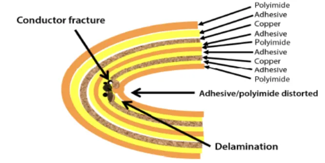
Cumulative effects from vias and overlaps exacerbate issues, as blind vias in multilayer flex alter local fields. Signal skew in differential pairs arises from asymmetric etching on flexible foils. Cost pressures limit material grades, pushing reliance on standard polyimides with broader epsilon tolerances. Qualification under IPC-6013E reveals failures in high-cycle bend tests where impedance drifts beyond specs. Engineers face trade-offs between electrical performance and mechanical endurance.
Practical Solutions and Best Practices for Flex PCB Impedance Control
Optimizing stackup forms the foundation of solutions for flex PCB impedance, starting with thicker dielectric cores to achieve lower target Z0 values like 50 or 90 ohms. Designers adjust trace widths and spacings iteratively using impedance calculators based on IPC-2141 principles, accounting for flex-specific parameters. Symmetric striplines provide stable shielding, while microstrips suit space-constrained areas. Early collaboration with fabricators refines tolerances to 10 percent or better through process controls. Simulation tools model hatched fills, targeting 50 to 70 percent density for balanced mechanical and electrical properties.
Hatched plane strategies mitigate bend-induced failures, with simulations predicting impedance shifts from hatch geometry. Uniform trace routing avoids bends over 90 degrees, adhering to IPC-2223E bend radius ratios based on copper ductility. Differential pairs benefit from edge-coupled configurations with tight spacing controls. Pre-production coupons enable TDR verification on representative sections. Multilayer designs laminate flex sections separately before rigid integration, preserving impedance profiles.
Verification integrates time-domain reflectometry and vector network analysis post-fabrication, correlating measurements to design models. Design rules specify minimum ground clearance and via stub lengths to minimize discontinuities. Material selection favors low-loss polyimides with consistent properties across batches. For rigid-flex, fanout traces gradually in transition zones. These best practices in impedance control flexible circuits yield robust designs.
Troubleshooting Common Issues in Flex PCB Impedance
Engineers often encounter impedance mismatches traced to coverlay misalignment, resolved by precise registration during lamination. Drift under thermal cycling points to adhesive outgassing, countered by low-moisture processes. Hatched plane resonances appear in S-parameter plots, fixed by adjusting fill patterns via field solvers. Bend cycle failures reveal copper fatigue, addressed by annealed foils per design standards. Systematic DFM reviews catch routing violations early. Case examples show 15 percent yield gains from iterative stackup tweaks.
Conclusion
Mastering flex PCB impedance control requires balancing electrical precision with mechanical flexibility through informed stackup design, optimized geometries, and rigorous verification. Challenges like material variability and bending effects demand proactive solutions rooted in standards and simulation. By implementing these strategies, electrical engineers achieve reliable high-speed performance in flexible PCB design. Key takeaways include early tolerance planning and hatched plane management. Future advancements in materials will further ease these demands, but current best practices suffice for demanding applications.
FAQs
Q1: What are the main challenges in flex PCB impedance control?
A1: Challenges flex PCB impedance arise from dielectric thickness variations, mechanical bending altering geometry, and hatched ground effects on field distribution. Manufacturing tolerances in thin films amplify trace width sensitivity. Solutions involve precise stackup modeling and TDR testing to maintain 10 percent tolerance. Adhering to IPC-2223E bend rules prevents dynamic shifts.
Q2: How does bending affect impedance control in flexible circuits?
A2: Bending compresses dielectrics, changing capacitance and thus Z0 in impedance control flexible circuits. Minimum bend radii per IPC-2223E guidelines mitigate this by preserving trace integrity. Hatched planes relieve stress but require simulation for impedance stability. Testing under flexed conditions verifies performance. Flexible PCB design must factor static versus dynamic use.
Q3: What are effective solutions for flex PCB impedance matching?
A3: Solutions for flex PCB include thicker cores, optimized trace dimensions, and 50 to 70 percent hatched fills. Field solver-based calculations per IPC-2141 ensure targets like 90 ohms. Stackup symmetry in striplines enhances shielding. Fabricator feedback refines tolerances. Post-build TDR confirms compliance.
Q4: Why is stackup critical for flexible PCB design impedance?
A4: Stackup dictates dielectric height and Er, directly impacting Z0 in flexible PCB design. Thinner flex layers demand wider traces for control, risking mechanical limits. Multilayer lamination sequences preserve uniformity. Early definition avoids respins. IPC-6013E qualification ties to stable construction.
References
IPC-6013E — Qualification and Performance Specification for Flexible/Rigid-Flexible Printed Boards. IPC, 2021
IPC-2223E — Sectional Design Standard for Flexible/Rigid-Flexible Printed Boards. IPC, 2020
IPC-2141 — Controlled Impedance Circuit Boards and High Speed Logic Design. IPC, 1996


