Introduction
In modern high-speed PCB designs, signal integrity challenges dominate as frequencies push into the GHz range. Vias, essential for multilayer interconnects, introduce discontinuities that degrade performance if not managed properly. The via stub effect becomes particularly pronounced, causing reflections and resonances that lead to high-frequency signal loss. Engineers must understand how stub length influences return loss, insertion loss, and eye diagram quality to meet stringent timing budgets. This article explores the via stub resonance mechanisms and practical strategies like backdrilling vias for mitigation. By minimizing via stub length, designers can achieve cleaner signal transmission in applications such as 5G infrastructure, data centers, and automotive radar systems.
Understanding Via Stubs in PCB Vias
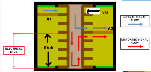
A via stub refers to the unused portion of a through-hole via extending beyond the signal trace's layer pair in a multilayer board. In through vias, which penetrate all layers, the stub acts as an open-ended transmission line when signals propagate at high frequencies. This creates the via stub effect, where the stub's impedance mismatches the controlled 50-ohm or 100-ohm lines, generating reflections that corrupt the waveform. As board stackups grow thicker for power and ground planes, stub lengths increase, amplifying the problem in designs above 5 GHz. Industry standards like IPC-2221 emphasize via design parameters to maintain signal integrity across layers. Addressing via stubs early in the design phase prevents costly respins and ensures compliance with performance specs.
The Mechanisms of Via Stub Resonance
Via stub resonance occurs when the stub length approaches a quarter-wavelength of the signal frequency, transforming it into a resonant circuit. At resonance, the stub reflects nearly 100% of the incident power back toward the source, severely distorting the transmitted signal. This phenomenon stems from transmission line theory, where the stub's input impedance drops to zero at λ/4, causing a voltage null and maximum reflection coefficient. For a 10 GHz signal with effective dielectric constant around 4, resonance might hit at stub lengths of 3-5 mm, depending on materials. High-frequency signal loss compounds as multiple vias compound reflections, leading to inter-symbol interference in serial links. Engineers model this using S-parameters, observing peaks in return loss (S11) corresponding to stub modes.
The via stub effect extends beyond resonance to continuous insertion loss from stub radiation and coupling to adjacent structures. Shorter wavelengths at higher frequencies make even modest stubs problematic, as the electrical length scales inversely with frequency. Precise stackup control and via placement spacing mitigate coupling, but stub length remains the primary culprit. Simulations reveal that a 2 mm stub can degrade eye height by 20-30% in 25 Gbps channels without correction.
Related Reading: A Deep Dive into PCB Via Stubs and Controlled Depth Drilling Solutions
Quantifying High-Frequency Signal Loss from Via Stubs
To assess the via stub effect, engineers evaluate key metrics like return loss, insertion loss, and crosstalk. A typical through via with a 10 mil stub at 10 GHz might exhibit 10-15 dB return loss peaks, unacceptable for most standards. Insertion loss increases due to stub-induced radiation, where energy leaks into the board rather than propagating forward. Time-domain reflectometry (TDR) traces show impedance bumps at the via transition, quantifying the discontinuity. Frequency-domain tools plot S21 dips aligning with stub resonances, guiding optimization efforts.
Factors influencing stub impact include via diameter, plating thickness, and pad size, all governed by fabrication tolerances. Thicker boards exacerbate longer stubs, pushing resonances lower in frequency. In controlled impedance environments, stubs disrupt differential pair balance, introducing common-mode noise. Data from vector network analyzer (VNA) measurements consistently links stub length to signal degradation thresholds.
Strategies for Minimizing Via Stub Length
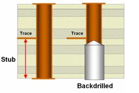
Minimizing via stub length starts with selecting appropriate via types during stackup planning. Blind and buried vias inherently reduce stubs by terminating at specific layers, ideal for dense high-speed boards. However, their fabrication complexity demands precise laser drilling and sequential lamination. Backdrilling vias offers a cost-effective alternative, mechanically removing the stub post-plating to leave only 0.5-1 mm residue. This technique preserves through connections while eliminating resonance sources, crucial for frequencies above 8 GHz.
Backdrilling vias requires careful specification of drill sizes and depths to avoid drill wander or breakout. Tolerances per IPC-6012 ensure reliability, with depth control within 0.1 mm for multi-layer boards. Designers pair this with via-in-pad or filled vias for further optimization, minimizing annular ring exposure. Simulation verifies post-backdrill performance, targeting return loss below -20 dB up to 20 GHz.
Alternative approaches include pressed or molded vias in advanced stackups, though less common due to yield concerns. Layer pairing strategies route signals within inner layers, using fewer transitions. Fabricators apply IPC-A-600 acceptability criteria to inspect backdrilled features for smear and plating voids.
Related Reading: The Impact of Controlled Depth Drilling on High Speed PCB Performance
Best Practices in Via Stub Management for High-Speed PCBs
Adopt a holistic design flow integrating electromagnetic simulation from schematic capture. Define via rulesets with maximum stub lengths based on frequency targets, such as under 1 mm for 25 Gbps. Optimize via aspect ratios below 10:1 to ease backdrilling and reduce inductance. Route critical nets with minimal via counts, preferring microvias for short hops.
Fabrication partners must support backdrilling with pilot holes and depth verification via x-ray or sectional analysis. Post-drill cleaning prevents residue-induced losses. Testing protocols include VNA sweeps and eye pattern analysis to validate via stub resonance suppression. Collaborate on stackup reviews to balance density, thermal management, and signal integrity.
In dense designs, stagger via grids to reduce crosstalk from stub fields. Ground via fencing around signals shields against radiation. These practices align with J-STD guidelines for high-speed assemblies, ensuring robust performance.
Real-World Insights: Troubleshooting Via Stub Issues
Consider a 12-layer board for a 10 Gbps Ethernet switch where initial prototypes showed eye closure at 9 GHz. Analysis pinpointed via stub resonance via VNA, with peaks at 8.5 GHz from 4 mm stubs. Implementing backdrilling on signal vias shifted resonances above 15 GHz, restoring 85% eye height. Pre-layout simulation would have flagged this, but fab iterations confirmed the fix. Similar issues in radar modules underscore proactive stub minimization. Lessons emphasize early modeling and standard-compliant via specs.
Conclusion
Via stub length profoundly impacts high-frequency signal integrity through reflections, resonance, and loss mechanisms. The via stub effect demands vigilant design, with backdrilling vias and advanced via types as proven remedies for minimizing via stub length. Engineers achieve reliable performance by quantifying effects via S-parameters and adhering to standards like IPC-2221 and IPC-6012. Integrating these strategies ensures signals propagate with minimal distortion in demanding applications. Prioritizing stub control from concept to fabrication yields robust, high-speed PCBs ready for future frequencies.
FAQs
Q1: What is the via stub effect and how does it cause high-frequency signal loss?
A1: The via stub effect arises from the unused via portion acting as a mismatched transmission line, reflecting signals at high frequencies. This leads to insertion and return loss, distorting waveforms and causing eye degradation. Resonance amplifies losses when stub length nears λ/4. Mitigation focuses on shortening stubs to preserve signal quality in GHz designs.
Q2: How does via stub resonance manifest in PCB measurements?
A2: Via stub resonance appears as sharp return loss peaks in S11 plots, typically every quarter-wavelength interval. TDR shows impedance discontinuities, while S21 dips indicate energy loss. Frequencies above 5 GHz reveal these clearly in multilayer boards. Simulations predict modes for design fixes.
Q3: What are effective methods for minimizing via stub length?
A3: Minimizing via stub length involves backdrilling vias to remove excess barrel, using blind or buried vias for layer-limited connections, and optimizing stackups for shorter paths. These reduce electrical length, suppressing resonance. Fabrication tolerances ensure clean results without reliability risks.
Q4: When should engineers consider backdrilling vias for signal integrity?
A4: Backdrilling vias suits designs exceeding 5-10 GHz where through-via stubs exceed 2 mm, causing unacceptable via stub resonance. It's cost-effective for production volumes and compatible with standard stackups. Verify via post-drill S-parameters to confirm high-frequency signal loss reduction.
References
IPC-2221B — Generic Standard on Printed Board Design. IPC, 2012
IPC-6012E — Qualification and Performance Specification for Rigid Printed Boards. IPC, 2015
IPC-A-600K — Acceptability of Printed Boards. IPC, 2020


