Introduction
Power distribution in printed circuit boards forms the backbone of reliable electronic systems, ensuring components receive stable voltage and current under varying loads. In modern designs, especially those incorporating system-on-chip modules and analog sensors, efficient power delivery prevents noise injection and performance degradation. For applications in industrial plants, where high reliability is paramount, robust power distribution networks mitigate risks from voltage fluctuations and thermal stress. This article explores the principles and practices for optimizing power distribution, focusing on how to layout PCB power supply designs effectively. Engineers must prioritize low impedance paths and adequate current handling to support dense, high-speed circuits. Adhering to established guidelines elevates design quality across performance classes.
What Is Power Distribution in PCB Design and Why It Matters
Power distribution refers to the network of conductors, planes, vias, and decoupling elements that deliver DC power from entry points to loads throughout the PCB. This power distribution network, or PDN, maintains voltage stability despite dynamic currents from switching components. In system-on-chip modules, which integrate multiple functions on a single die, the PDN must handle localized high currents without excessive drop. Analog sensors, sensitive to supply noise, demand clean power rails to preserve signal accuracy in noisy environments like industrial plants. Poor PDN design leads to ground bounce, EMI radiation, and premature failures, increasing system costs. Thus, effective power distribution directly impacts signal integrity, thermal management, and overall board reliability.
Industry relevance amplifies in high-power scenarios, where voltage regulators feed multiple rails amid compact layouts. Compliance with standards like IPC-2221 ensures designs meet performance requirements for conductor spacing and layer stackups. Neglecting PDN optimization can cascade into assembly issues or field failures, underscoring its foundational role.
Key Technical Principles of Power Distribution
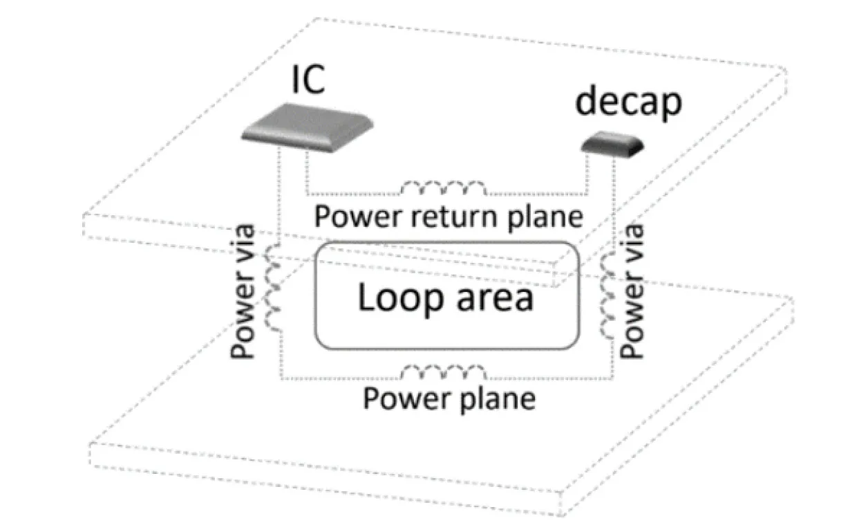
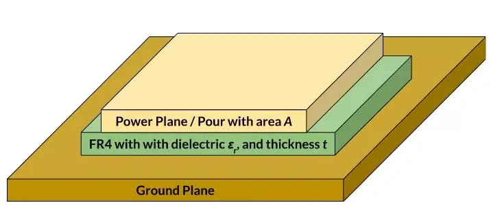
The core principle of power distribution centers on minimizing impedance across frequency ranges, from DC to GHz, to keep voltage ripple below component tolerances. Solid power and ground planes provide the lowest inductance paths, distributing current evenly and reducing loop areas for return currents. In multilayer boards, dedicating inner layers to power reduces trace lengths and crosstalk with signals. Current density limits, governed by IPC-2152, dictate trace widths and plane thicknesses to prevent overheating, with external traces heating faster than internal ones due to convection differences. Vias serve as vertical interconnects, but arrays or stitching prevent bottlenecks at plane transitions.
Decoupling capacitors bridge frequency gaps, shunting high-frequency noise locally while bulk caps handle low-frequency demands. Plane splits require careful bridging to avoid high-impedance discontinuities that amplify noise. For analog sensors, separate analog and digital power domains isolate sensitive circuits from switching noise. These mechanisms collectively form a resilient PDN, scalable to industrial plant demands.
How to Layout PCB Power Supply Designs: Best Practices
Start by defining power entry points near voltage regulators, using wide traces or planes sized per IPC-2152 current charts for the maximum expected load. Place regulators close to high-current loads like system-on-chip modules to minimize distribution losses, routing power traces first before signals. Employ full or split planes for rails, ensuring ground planes adjoin power layers for tight coupling and low inductance. Via stitching along plane edges maintains equipotential across splits, with density increasing near high-frequency components.
Position decoupling capacitors within millimeters of IC power pins, prioritizing low-ESL ceramics in pi-filters for broadband suppression. For analog sensors, route dedicated power traces with guards or moats to shield from digital returns, filtering at the rail origin. In industrial plants, incorporate redundancy like parallel paths or thicker copper to handle fault currents. Simulate PDN impedance early, targeting below 1/(load current * ripple voltage) across frequencies. Layer sequencing follows IPC-2221, alternating power-ground pairs outward from core signals. These steps yield layouts resilient to real-world stresses.
Flood pours over unassigned areas connect to ground, stabilizing references and aiding manufacturability. Star-point grounding converges returns at a single low-impedance node, preventing loops in mixed-signal boards. Thermal vias under power devices dissipate heat, complementing PDN sizing.
Challenges and Troubleshooting in Power Distribution
Voltage droop under transient loads signals insufficient decoupling or long paths; measure with scope probes and add caps iteratively. Hotspots from current crowding appear in simulations or IR scans, resolved by widening constrictions or adding planes. Noise coupling between split planes couples via slots, fixed by stitching or overlap bridges. In system-on-chip modules, pinout constraints demand careful rail pairing to balance currents.
Industrial plants expose boards to vibrations, prompting reinforced vias and J-STD-001 compliant solder joints for mechanical integrity. EMI failures trace to long power loops; shorten with planes and ferrite beads. Troubleshooting involves peel-back analysis: isolate sections, measure ripple, and correlate to layout flaws. Proactive stackup planning averts most issues.
Conclusion
Mastering power distribution PCB design hinges on low-impedance networks tailored to component demands, from system-on-chip modules to analog sensors. Best practices in plane usage, decoupling, and sizing per standards like IPC-2152 and IPC-2221 ensure stability in demanding industrial plants. Logical layout sequencing and simulation verify performance before fabrication. Engineers achieve reliable how to layout PCB power supply designs by balancing electrical, thermal, and manufacturability factors. Prioritizing PDN elevates overall board quality, reducing iterations and field issues.
FAQs
Q1: What are the main steps in how to layout PCB power supply designs?
A1: Begin with power entry sizing per current needs, dedicate planes for low impedance, and place regulators near loads. Add via stitching at splits and decoupling caps at pins. Simulate impedance to confirm margins. This structured approach suits system-on-chip modules and industrial plants, aligning with IPC-2221 guidelines for robust performance.
Q2: How does power distribution affect analog sensors on PCBs?
A2: Analog sensors require isolated, low-noise rails to avoid distortion from digital switching. Use separate planes with filters and guards in layouts. Proper PDN minimizes ripple, preserving accuracy in noisy environments like industrial plants. Follow IPC-2152 for trace capacities to prevent drops.
Q3: Why use power planes in PCB power supply designs for industrial plants?
A3: Planes offer uniform current spread, low inductance, and EMI shielding essential for high-reliability applications. They outperform traces in handling surges and heat. Stitch vias ensure continuity across layers. This practice supports demanding loads in system-on-chip modules per industry standards.
Q4: What role does IPC-2152 play in power distribution layouts?
A4: IPC-2152 provides charts for trace and plane sizing based on current, temperature rise, and copper weight. It guides how to layout PCB power supply designs to avoid overheating. Internal layers allow higher densities than externals. Essential for thermal-safe PDNs in dense boards.
References
IPC-2221C — Generic Standard on Printed Board Design. IPC, 2019
IPC-2152 — Standard for Determining Current Carrying Capacity in Printed Board Design. IPC, 2009
J-STD-001J — Requirements for Soldered Electrical and Electronic Assemblies. IPC, 2024


