Introduction
In modern electronics, printed circuit boards handle increasing power densities from advanced components like processors and power converters. Effective thermal management ensures these designs operate reliably without degradation. Overheating leads to reduced lifespan, performance drops, and potential failures in critical applications. Engineers must integrate thermal analysis in PCB design early to identify hotspots and implement cooling techniques. This article explores PCB thermal simulation software, thermal vias for PCBs, heat sink selection for PCBs, and other PCB cooling techniques. By understanding these tools, designers can prevent PCB overheating and optimize system efficiency.
Why Thermal Management Matters in PCB Design
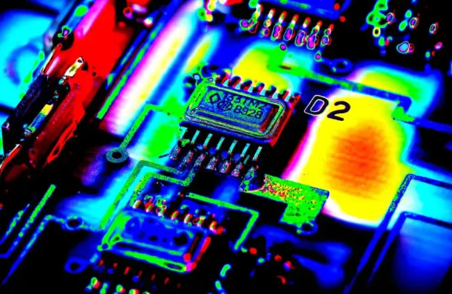
Heat generation in PCBs arises from resistive losses in traces, dielectric heating, and component junction temperatures. Without proper thermal management, junctions exceed safe limits, causing electromigration or delamination. Industry demands compact layouts with high-speed signals, amplifying thermal challenges. Thermal analysis in PCB design reveals how heat flows through layers and to the environment. Neglecting this risks non-compliance with performance specs and increases field failures. Prioritizing thermal management tools comparison helps select approaches that balance cost, space, and effectiveness.
Reliability standards emphasize thermal considerations during design phases. For instance, guidelines in IPC-2221 address heat dissipation strategies to maintain board integrity. Engineers benefit from structured evaluations to predict real-world behavior under load.
Fundamentals of Heat Transfer in PCBs
Heat transfer in PCBs occurs primarily through conduction within materials, convection to air, and radiation, though radiation plays a minor role at typical temperatures. Copper layers offer high thermal conductivity, spreading heat laterally, while substrates like FR4 limit vertical transfer due to lower values. Understanding PCB material thermal conductivity guides layer stackup choices for better dissipation. Thermal gradients cause mechanical stresses from coefficient of thermal expansion mismatches between copper and dielectrics.
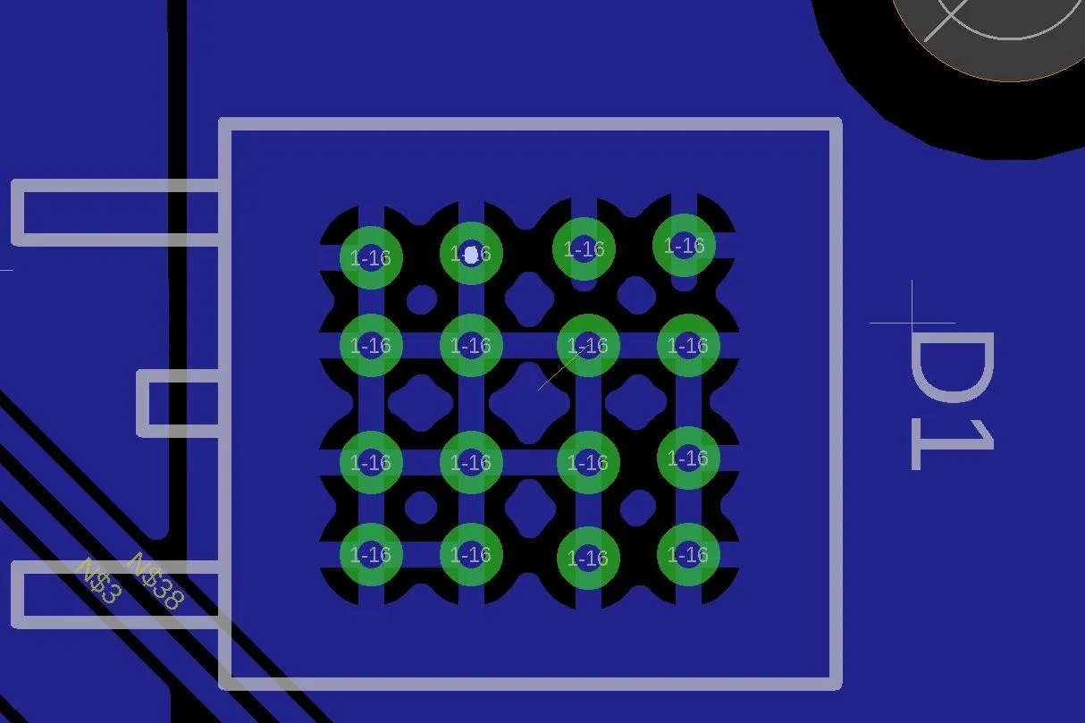
Vias bridge layers, acting as thermal conduits when filled or plated appropriately. Arrays of thermal vias for PCBs enhance paths from surface components to inner planes. Convection relies on airflow over board surfaces, influenced by finned structures or enclosures. Engineers model these mechanisms to forecast temperatures accurately.
Key Thermal Management Techniques
Thermal Vias for PCBs
Thermal vias transfer heat vertically through the board stackup, connecting hot components to lower-temperature planes. Designers place them in arrays under power devices, with spacing optimized for density without compromising electrical isolation. Plating thickness affects conductance, and filling options improve performance in high-reliability builds. As noted in IPC-2221, thermal vias are recommended under high-power devices to manage localized heating.
Effective implementation involves balancing via count with fabrication limits, ensuring annular rings prevent shorts. These structures integrate seamlessly with copper pours for lateral spreading. Testing validates models by measuring temperature drops across layers.
Related Reading: Thermal Via Stitching: Cooling Your High Power PCBs
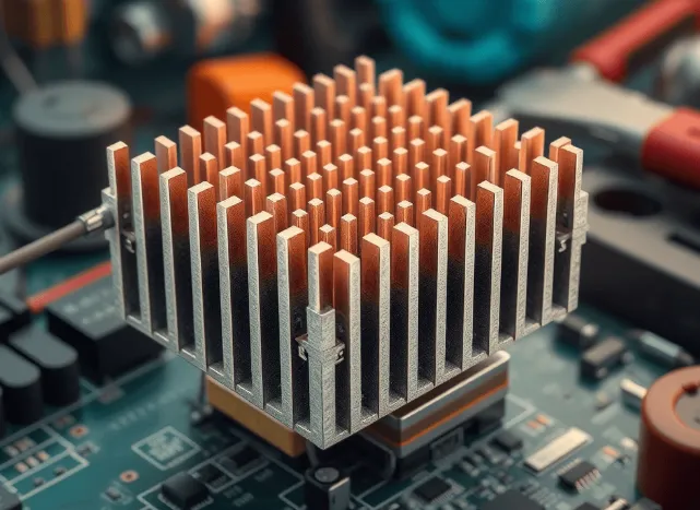
Heat Sink Selection for PCBs
Heat sinks attach to components or board surfaces, increasing surface area for convection. Selection considers thermal resistance, footprint, and attachment method like clips or thermal interface materials. Fin geometry, density, and orientation optimize airflow, whether natural or forced. Engineers calculate required dissipation based on power input and ambient conditions to avoid oversizing.
Material choice favors aluminum for cost or copper for superior conductivity, weighed against weight constraints. Interface gaps must minimize with pads or grease for low resistance. Integration requires board-level planning to accommodate height and secure mounting.
Related Reading: Thermal Vias and Heat Sinks: Keeping Avionics System PCBs Cool Under Pressure
High Thermal Conductivity Materials
PCB material thermal conductivity varies significantly, with standard laminates offering modest through-plane values but better in-plane performance. Advanced dielectrics or metal-backed cores provide pathways for demanding applications. Stackups position high-conductivity layers near heat sources to shorten paths. IPC-4101 specifications classify materials by thermal properties, aiding selection for multilayer boards.
Hybrid constructions combine organics with embedded metals for targeted cooling. Designers evaluate total stackup impedance to heat flow during layout.
PCB Thermal Simulation Software and Analysis
PCB thermal simulation software models steady-state and transient behaviors, predicting temperatures from geometry and boundary conditions. Inputs include material properties, power maps, and airflow profiles for accurate thermal analysis in PCB design. Iterative simulations refine layouts before prototyping, saving time and cost. Mesh refinement focuses on hotspots for computational efficiency.
Comparisons of simulation approaches reveal trade-offs in solver speed versus precision. Coupled electro-thermal models account for self-heating in traces. Validation against measurements ensures reliability in production.
- Thermal Vias for PCBs: Pros: Low cost, integrated; Cons: Limited vertical capacity; Best for: Multilayer power boards.
- Heat Sink Selection for PCBs: Pros: High dissipation; Cons: Adds height, cost; Best for: Discrete high-power components.
- High Conductivity Materials: Pros: Passive, board-level; Cons: Higher material expense; Best for: Compact, high-density designs.
- PCB Thermal Simulation Software: Pros: Predictive, iterative; Cons: Learning curve, compute time; Best for: Complex, pre-prototype analysis.
This thermal management tools comparison highlights selection based on design constraints.
Best Practices for Preventing PCB Overheating
Start with component placement, grouping heat sources apart and near edges for airflow. Wide traces and pours under devices spread heat early. Incorporate multiple ground planes as heat sinks internally. Layer sequencing places power on outer layers for direct cooling.
During layout, run thermal analysis in PCB design to iterate vias and copper. Specify via tents or fills for protection. Enclosure design complements board-level efforts with vents or fans. Post-fabrication, infrared imaging verifies performance.
Prototype testing under worst-case loads confirms margins. Documentation includes thermal profiles for downstream assembly.
Advanced PCB Cooling Techniques
Beyond basics, embedded heat pipes or vapor chambers handle extreme densities. Microchannel structures in substrates enhance convection internally. Active cooling like integrated fans suits enclosed systems. Hybrid approaches combine passive elements with simulation-driven optimization.
Preventing PCB overheating demands holistic design, from schematic to enclosure. Regular reviews align with evolving component powers.
Conclusion
Thermal management tools empower engineers to maintain PCB integrity under pressure. From thermal vias for PCBs and heat sink selection for PCBs to PCB thermal simulation software, each technique addresses specific challenges. Integrating PCB cooling techniques and focusing on PCB material thermal conductivity ensures robust designs. Thermal analysis in PCB design prevents failures proactively. By following structured practices and standards, teams deliver reliable, efficient boards ready for demanding environments.
FAQs
Q1: What role does PCB thermal simulation software play in design?
A1: PCB thermal simulation software predicts hotspot formation and temperature profiles across the board. It allows engineers to test PCB cooling techniques virtually, optimizing layouts before fabrication. This reduces iterations and ensures compliance with thermal limits, enhancing overall reliability in high-power applications.
Q2: How do thermal vias for PCBs improve heat dissipation?
A2: Thermal vias conduct heat from surface components to inner copper planes efficiently. Arrays under hotspots create low-resistance paths, complementing lateral spreading. Proper sizing and density, per design guidelines, maximize effectiveness without electrical interference, which is crucial for multilayer boards.
Q3: What factors influence heat sink selection for PCBs?
A3: Heat sink selection depends on thermal resistance needs, available space, and airflow type. Engineers match fin design to power dissipation and ambient conditions for optimal performance. Secure attachment minimizes interface resistance, ensuring efficient heat transfer in compact assemblies.
Q4: Why is PCB material thermal conductivity important?
A4: PCB material thermal conductivity determines how effectively heat moves through the stackup. Higher values reduce gradients and hotspots, which is vital for dense designs. Selecting materials per specifications supports preventing PCB overheating and maintains signal integrity alongside thermal goals.
References
IPC-2221 — Generic Standard on Printed Board Design. IPC
IPC-2152 — Standard for Determining Current Carrying Capacity in Printed Board Traces. IPC
IPC-4101 — Specification for Base Materials for Rigid and Multilayer Printed Boards. IPC


