 00:53
00:53
NSMD Pads
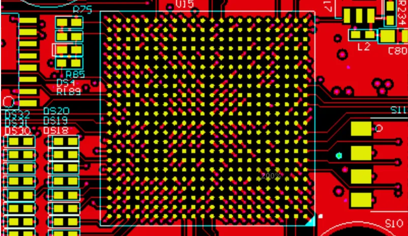
Non Solder Mask Defined (NSMD) pads represent a critical design choice in printed circuit board (PCB) manufacturing, where the solder mask opening extends beyond the copper pad edges. This configuration allows the solder to flow more freely during assembly, enhancing joint reliability and reducing the risk of defects such as tombstoning or bridging. Engineers and designers often search for information on NSMD pads when optimizing PCB layouts for high-density applications, such as in consumer electronics, automotive systems, or telecommunications equipment. Understanding NSMD pads is essential for achieving better solderability, especially with fine-pitch components like ball grid arrays (BGAs) and quad flat no-leads (QFNs), where precise control over solder mask clearances can significantly impact overall board performance and yield rates. In practice, implementing NSMD pads involves careful consideration of factors like pad size, mask expansion, and material compatibility to prevent issues such as pad lifting or insufficient solder volume. Best practices include maintaining a mask clearance of 0.05 to 0.075 mm around the pad to promote optimal solder wetting while avoiding exposure of underlying traces. This approach not only improves mechanical strength but also facilitates easier rework and inspection processes. For those troubleshooting assembly failures or seeking to comply with industry standards like IPC-7351, articles tagged under NSMD Pads offer valuable insights into design guidelines, simulation techniques, and real-world case studies that demonstrate how to integrate these pads effectively into your projects. Readers interested in advancing their PCB design skills will find a range of detailed discussions in our related content, covering topics from initial layout strategies to advanced fabrication methods. By exploring these resources, you can gain practical knowledge to refine your designs and address common challenges in electronics manufacturing.
Video Guide
-
00:53
Technical Articles