










PCB Solder Mask Bridges Issues: Fine-Pitch DFM
Key Moment
What This Video Covers
This engineering-review video explains why a CAM team asks about solder mask bridges even when copper DRC is clean. Default solder mask expansion opens each pad slightly larger than copper. When two openings meet in a tight gap, the remaining web, the solder mask dam, can fall below process capability and flake, merge, or vanish.
Four production cases walk through the decision: opening the mask between fine-pitch SMT pads at 5 mil and 2 mil copper clearance; switching a dense NSMD BGA toward SMD pads when pad-to-pad clearance drops below about 7.8 mil; tightening limits for red, yellow, black, or white mask and for 2 oz copper versus 1 oz green or blue; and the reverse call, adding a dam back when a gang opening is unnecessary, or clearing gold-finger areas instead.
The same rules apply to HDI PCB layouts, 4 layer PCB and 6 layer PCB prototypes, and high-density PCB assembly for QFP, QFN, BGA, and connector fields. Review mask layers and pad-to-pad spacing before you request a PCB quote or PCBA quote, then let CAM confirm the dam against real ink, color, and copper capability.
Key Highlights
- A solder mask dam is the web left after both pad openings expand; copper clearance alone does not prove the dam will survive imaging.
- At 5 mil (and locally 2 mil) pad spacing, factories often recommend a merged opening rather than a sliver that cannot be formed reliably.
- NSMD BGA openings below about 7.8 mil pad-to-pad can erase dams entirely; SMD pads, mask color, and copper weight (1 oz vs 2 oz) change the minimum that can be held.
What a Solder Mask Dam Is and Why Expansion Shrinks It
Layout tools expose copper for soldering by applying a default solder mask expansion. The opening is drawn larger than the land so registration error does not leave ink on the pad. That expansion is applied from both sides of every gap. What remains between two openings is the dam, also called a solder mask bridge or sliver.
The dam is a fabrication feature, not an assembly defect. If it is too thin, LPI ink may not image, develop, and adhere. A broken sliver can lift in develop or wash and leave two openings that behave as one. During reflow, molten solder then has no physical barrier. That is why the EQ arrives as "the IC's pad spacing is too small to form a solder mask dam," not as a copper short.
Designers who only inspect the copper layer miss the problem. The solder mask Gerber (typically GTS/GBS) is the layer that must be measured after expansion. If that remaining width is below the fabricator's capability for the chosen color and copper weight, CAM will propose a merged opening, a reduced expansion, or a change from NSMD to SMD.

Case 1: Fine-Pitch SMT Pads That Cannot Keep a Dam
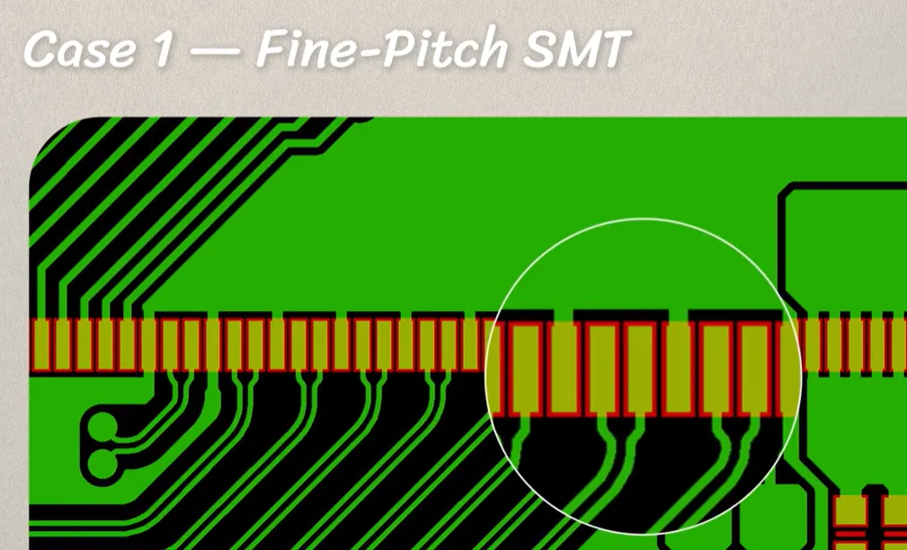
In the first production case, copper pad-to-pad clearance on a fine-pitch SMT package was 5 mil and locally only 2 mil. After standard expansion, the remaining dam was below process capability. Trying to keep that sliver would produce incomplete coverage, lifted ink, or an unreliable web that would not survive develop.
The factory recommendation was to open the solder mask between the pads, a gang or merged opening, rather than force a dam the process cannot hold. That choice trades a physical barrier for a controlled, continuous window. Assembly then depends on stencil aperture design, paste volume, and reflow profile rather than on a mask wall that would not exist on the finished board.
This pattern is common on QFP and QFN rows, connector pins, and 01005/0201 clusters on consumer electronics PCB and industrial control PCB designs. If the package footprint was imported with a generic 3-4 mil expansion, the dam math fails even when copper-to-copper DRC is green.
Case 2: NSMD BGA Arrays Where Dams Disappear
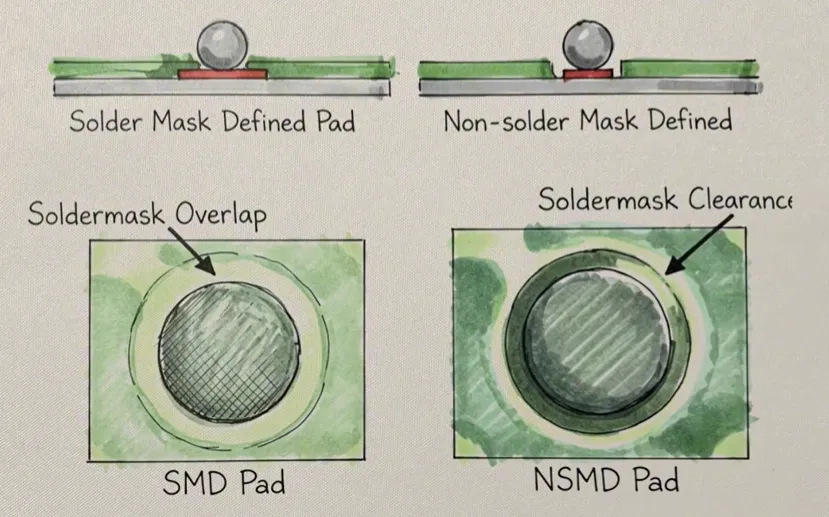
NSMD pads use a mask opening larger than the copper land so the entire pad edge is available for wetting. That is good for joint strength and thermal cycling on many BGA pitches. It is costly for dam width. Each opening consumes extra gap. When pad-to-pad clearance falls below about 7.8 mil, adjacent openings can leave almost no web, or none at all across a dense array.
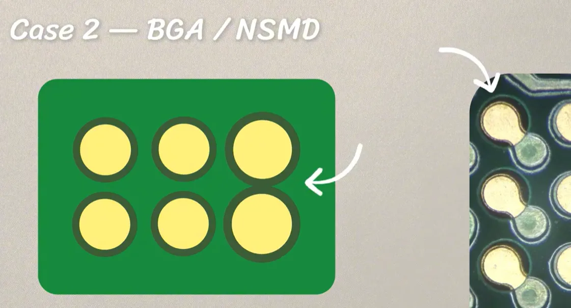
Without a dam, there is no mask wall between balls. Solder bridging risk rises during reflow, especially with paste misregistration or excess volume. When a dam must be retained, CAM may recommend Solder Mask Defined (SMD) pads: the opening is equal to or smaller than the copper, so the mask edge defines the land and a wider web can be kept between balls.
NSMD remains the better default for many 0.8 mm and 1.0 mm pitches. SMD becomes the practical option as pitch tightens toward 0.5 mm and below, or when via-in-pad and HDI PCB fanout leave no spare mils. Do not mix SMD and NSMD inside one BGA without a thermal and collapse analysis; mixed definition changes wetting area and can lift the package on one side of the array.
Case 3: How Mask Color and Copper Weight Change Minimum Spacing
Spacing is not a single number. Ink chemistry, pigment loading, and copper topography change the minimum dam that will image cleanly.
The video cites typical CAM guidance:
| Copper weight | Green / blue mask | Red / yellow / black / white |
|---|---|---|
| 1 oz | ~7.8 mil pad-to-pad for a reliable dam | up to ~9.8 mil |
| 2 oz | ~9.08 mil even for green / blue | still tighter than 1 oz green; confirm with CAM |
Green and blue formulations are usually the most UV-responsive and can hold a narrower web. Red, yellow, black, and white often need a wider dam because pigments reduce exposure latitude and adhesion on a thin sliver. Two-ounce copper raises the pad step height. Mask thins over the copper corner and the web between tall pads is harder to keep continuous.
A clearance that passed on a 1 oz green prototype can fail on a 2 oz black production revision. Treat color and finished copper as DFM inputs, not cosmetics. If branding requires white or black on a fine-pitch automotive PCB or telecommunication PCB, either relax pitch, switch selected lands to SMD, or accept a gang opening in the tightest rows.

Case 4: When CAM Adds a Dam Back, or Opens a Gang Window
Not every EQ removes the dam. In some files the customer already merged openings. If CAM measures a remaining web that the process can hold, and if a dam would improve assembly isolation, the factory may recommend putting the dam back.
The opposite call appears on gold fingers and some connector rows. A continuous gang opening can be cleaner for plating, bevel, and contact wipe than a series of fragile dams. The rule is local: keep the dam where it is manufacturable and useful; open the window where the dam would be a sliver or would interfere with plating and mating surfaces.
This is why "compare your design to the manufacturer's capability and look at the solder mask layers, not only copper" is the closing instruction. CAM is not automatically deleting features. It is matching the remaining web to ink, color, copper, and the assembly risk of that package.

SMD vs NSMD Pad Choice When the Dam Is at Risk
| Decision factor | Prefer NSMD | Prefer SMD |
|---|---|---|
| Typical pitch | ≥ ~0.5-0.8 mm BGA | Ultra-fine pitch; dam must exist |
| Mask opening vs copper | Opening larger than land | Opening ≤ land |
| Dam width after expansion | Consumes more of the gap | Easier to retain a web |
| Joint / reliability | Larger wetting area, often better fatigue | Stronger mask anchor; higher void risk if poorly designed |
| Registration | More tolerant of mask shift on the pad | Mask alignment is critical |
| When CAM flags the dam | Reduce expansion or accept gang open | Convert lands so a dam can be formed |
Use NSMD when the gap after expansion still meets the color/copper table. Use SMD when the array cannot keep a web and bridging risk is unacceptable. Confirm stencil apertures after either change so paste volume still matches the new exposed copper.
Pre-Release Checklist for Solder Mask Layers
- Measure pad-to-pad copper and remaining mask web after the actual expansion rule.
- Inspect GTS/GBS, not only the 3D viewer or copper DRC.
- Flag QFP, QFN, BGA, and connector fields first.
- Recalculate if you change mask color or finished copper (1 oz vs 2 oz).
- Decide per region: keep dam, reduce expansion, convert NSMD to SMD, or gang-open.
- Treat gold fingers as a separate rule set.
- Send the question with the Gerbers if the web is near the limit. Do not wait for a hold.
A PCB prototype run is the cheapest place to validate the dam. For volume, lock color, copper weight, and pad definition before PCB mass production so CAM does not change the land pattern after qualification.
FAQ
Q1: If copper DRC passed, why is the manufacturer still asking about solder mask bridges?
A1: Because the dam is measured after solder mask expansion on the mask layer. Two lands can clear copper-to-copper and still leave a web thinner than the ink can form for that color and copper weight.
Q2: When should I accept a gang solder mask opening instead of keeping the dam?
A2: When pad-to-pad clearance after expansion is below process capability (the video examples include 5 mil and 2 mil copper gaps on fine-pitch SMT). A forced sliver is less reliable than a planned merged window plus a controlled stencil.
Q3: At what BGA clearance do NSMD dams typically fail?
A3: The case in this video uses about 7.8 mil pad-to-pad as the point where NSMD openings leave little or no dam. Below that, SMD pads or a reduced expansion are the usual CAM options. Confirm against your fabricator's table. Color and 2 oz copper raise the number.
Q4: Does switching from green to black or white mask force a respin of fine-pitch footprints?
A4: Often yes. The video cites ~7.8 mil for 1 oz green/blue versus up to ~9.8 mil for red, yellow, black, or white, and ~9.08 mil for 2 oz even on green/blue. Changing color on a tight QFN or BGA can turn a passing dam into an EQ.
Q5: Will CAM always remove the dam if they send an EQ?
A5: No. If a customer merged openings but the dam is still manufacturable and helps assembly, CAM may recommend adding it back. Gold-finger and some connector areas may be opened on purpose. The EQ is a capability check, not a single edit.
When your design includes fine-pitch components, you may receive a message from your PCB manufacturer:
"The IC's pad spacing is too small to form a solder mask dam."
But what exactly is a solder mask dam? And why would the factory flag it?
Here are some real production cases to show what can go wrong when a solder mask dam is too narrow—and how these issues are handled before production.
To ensure the copper pad is fully exposed for soldering, PCB layout software applies a default "solder mask expansion." This means the solder mask opening is intentionally made slightly larger than the copper pad itself.
When two adjacent pads are close together, this expansion eats into the gap from both sides. What remains between the two openings is the solder mask dam.If that dam becomes too thin, the manufacturer may no longer be able to form it reliably during production.
Case 1 — Fine-Pitch SMT
Here's our first real production case.
Take a fine-pitch SMT component where the copper pads are exceptionally close. In this case, the pad-to-pad clearance was only 5 mil—and in some tight areas, it dropped to just 2 mil.
When the standard solder mask expansion is applied, the space left between the two mask openings becomes extremely narrow. What remains is the solder mask dam.
But at such a small clearance, the remaining solder mask can fall below the manufacturer's process capability, making the dam difficult to form and maintain reliably during production.
So in this case, the manufacturer recommended opening the solder mask between the pads instead of trying to retain the dam.
Case 2 — BGA / NSMD
The second case shows how this same issue can become even more challenging in a high-density BGA array using Non-Solder Mask Defined, or NSMD, pads.
With NSMD pads, the solder mask opening is intentionally larger than the copper land. So when the pad-to-pad clearance drops below 7.8 mil, there may be virtually no room left for a reliable solder mask dam between adjacent openings.
In a dense BGA array, the dams can disappear altogether.
Without a dam, there is no physical barrier between adjacent openings, which can increase the risk of solder bridging during reflow.
When retaining the dam is required, the manufacturer may recommend using Solder Mask Defined (SMD) pads as an alternative approach.
Case 3 — Color, Copper, and Process Limits
But spacing isn't the only factor.
Solder mask color and copper thickness can also change the minimum pad-to-pad spacing.
For example, with 1 oz copper, green or blue mask requires around 7.8 mil, while red, yellow, black, or white can require up to 9.8 mil.
And with 2 oz copper, even green or blue can require around 9.08 mil.
So a clearance that works for one combination may not be enough for another.
Case 4 — When the Manufacturer Asks You to Confirm
But CAM review doesn't always mean removing the dam.
In some cases, a customer's design uses a merged gang opening, but our engineers find that the dam can still be reliably maintained.
If it benefits assembly, we may recommend adding the dam back.
And in special areas like gold fingers, the decision can go the other way—we may recommend a clear gang opening instead.
If you're working with fine-pitch QFPs, QFNs, BGAs, connectors, or other dense SMD areas, it's worth taking a little extra time to check your solder mask design.Before you send your files, take a quick look at your pad-to-pad spacing and solder mask expansion. Make sure your openings won't merge, and check the solder mask layers—not just the copper layout.Also consider your solder mask color and copper thickness, as both can affect the manufacturer's spacing capability. It's also a good idea to compare your design with your manufacturer's capabilities and give the Gerbers a final look, especially around fine-pitch components.
Of course, you can check these points yourself before sending your files. And if something still needs adjustment, don't worry—your manufacturer's CAM team can catch it during review and suggest the necessary changes before production.
Hopefully, this gives you a better idea of what happens during PCB manufacturing.If you have a PCB project of your own, feel free to check out our profile.We also have a new-customer offer available for your first order.





