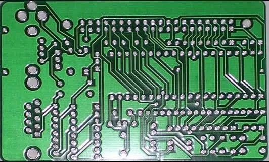
A visible gap between pad copper does not mean the finished board will keep a solder mask bridge. Solder-mask openings expand by rule. After the two openings overlap, the remaining mask still has to pass the fabricator's minimum solder-dam width, registration tolerance, and exposure capability. The decision belongs on the final solder-mask Gerber, not on the copper layer alone.
In the layout the two pads clearly do not touch, yet after Gerber export the entire mask between them is opened, or the fabricator reports that a solder mask bridge cannot be kept. The software did not draw the copper incorrectly. Copper clearance and solder-mask opening were treated as the same dimension. The judgment is explicit: whether a solder mask bridge can be kept depends on the net remaining width after both openings expand and on the fabricator's process limits.
Measuring pad-edge-to-pad-edge spacing at most proves that the copper is not shorted. It does not prove that the solder-mask layer still has enough material, and it cannot replace a check of the finished files.
1. Copper Has a Gap. Why Can the Solder Mask Still Become One Opening?
In most EDA tools and manufacturing files, the solder-mask layer is expressed as openings: where graphics exist, solder mask should not cover. To keep mask from overlapping the solderable surface, the opening is usually enlarged beyond the copper pad. Each of the two pads expands once toward the center, and a copper gap that looked generous is consumed twice.

Copper clearance is therefore only the geometric starting point. What actually decides the solder mask bridge is how much mask remains between the openings. If the two openings intersect, the output file forms one continuous aperture, and the fabricator has no mask strip left to keep.
2. Software Rules Pass. Why Can the Fabricator Still Remove the Bridge?
EDA only generates graphics from the expansion value you give it. It does not know how narrow a solder dam the specific factory can hold stably at the current board thickness, ink, surface finish, and pad density. Even if a thin line remains on the drawing, exposure registration and ink adhesion may still make it unstable in volume production.

When a fabricator asks to delete an undersized solder-mask bridge, the intent is to reduce the risk of a broken dam, misregistration, or residual mask. There is no universal safe number detached from process. Minimum solder-dam width and opening compensation must be confirmed with the actual supplier and written into that project's capability table.
3. Do Not Mix the Solder-Mask Layer and the Stencil Layer When You Edit
- Solder-mask opening: decides where mask covers, and affects pad exposure and bridge width.
- Stencil aperture: decides printed solder-paste area, serves paste volume and reflow, and is not solder mask.
- Copper pad: carries the electrical connection and the solderable surface. Changing it affects current, heat, and package size.
When bridge width is insufficient, shrinking the stencil does not bring the mask back. Blindly shrinking copper may also break the package soldering window. First confirm which layer's boundaries are overlapping, then decide whether to adjust solder-mask expansion, accept a merged opening, or change to a more manufacturable package and pitch.

4. Before Release, Check One Single-Variable Chain
Keep pad copper size fixed and change only the solder-mask expansion. Export two solder-mask Gerber versions. Zoom the same pad pair to pixel level and measure the remaining strip between the two openings. That shows whether the problem comes from the opening, not from copper clearance.

- In the footprint library, confirm whether solder mask follows a global rule, a local override, or a hard-coded value.
- In a CAM or Gerber viewer, overlay copper and solder mask and measure the final net width.
- Map that net width item by item against this fabricator's minimum solder dam, registration capability, and special process requirements.
- If a merged opening is the only option, state the accepted boundary in the assembly notes and separately review stencil and soldering risk.
A solder mask bridge does not appear automatically just because copper shows a gap. It must pass three constraints: opening expansion, overlap from both sides, and manufacturing capability. If any one of them is undefined, a green DRC check mark cannot guarantee the finished board.
The next time dense pads are reviewed, open the solder-mask Gerber directly. Are you measuring copper clearance, or the strip of mask that actually remains after the openings?
In your current footprint library, is solder-mask expansion a global rule or a pad-level override?