This situation is common: the board comes back, signal quality is poor during test, EMC fails outright, and only during the rework does it become clear that the stackup was wrong from the start.
That is how many engineers first get caught. A 4-layer board seems sufficient, the layers are assigned casually, and three boards in a row fail signal integrity testing. On the fourth board, looking at the stackup drawing, the problem is obvious: the return path is broken, so the board was never likely to work.
That is the point at which it becomes clear that a PCB stackup is not simply "splitting layers." It is the foundation of the entire PCB design. If the stackup is wrong, later optimization of signal routing will not recover the design.
First, Clarify What Layers a PCB Has
A standard 4-layer structure looks like this:
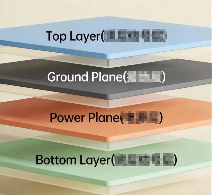
From top to bottom:
- Top Layer (top signal layer): mainly high-speed signals and critical components
- Ground Plane: a continuous ground plane that provides a low-impedance return path
- Power Plane: a 3.3 V / 5 V or similar power plane that can also serve as a reference plane
- Bottom Layer (bottom signal layer): low-speed signals and general routing
Core principle: signal layers must be separated by a continuous plane. That is the first line of defense for signal quality.
A Mistake Made by 90% of Beginners
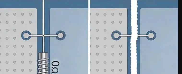
The following comparison shows a pitfall that is easy to encounter:
Incorrect approach (right side of the figure):
- Signal layer adjacent to signal layer
- No continuous ground plane
- Power plane heavily broken up
Correct approach (left side of the figure):
- Signal-plane-signal alternating arrangement
- A continuous ground plane is maintained
- The power plane is kept as continuous as possible
Why This Matters
When a high-speed signal is routed on the Top Layer, its return current automatically seeks the lowest-impedance path. If a continuous ground plane is directly underneath, the return current flows tightly under the signal trace and forms the shortest return path.
If another signal layer is underneath instead, the return current has to take a longer route. That leads to:
- Increased loop inductance → degraded signal quality
- Radiated interference → EMC test failure
- Crosstalk noise → higher bit error rate
Practical Method for Designing a Reasonable Stackup
Based on experience, a practical stackup design method can be summarized as follows.
1. Determine the Layer Count
| Application | Recommended layers | Reason |
|---|---|---|
| Simple low-speed circuits (<50 MHz) | 2 layers | Cost first, routing is simple |
| General digital circuits (50–200 MHz) | 4 layers | Best cost-performance balance |
| High-speed circuits (200 MHz–1 GHz) | 6 layers | Needed to maintain signal integrity |
| High-frequency, high-speed (>1 GHz) | 8 layers or more | Multiple power planes and differential pairs are required |
2. Layer Assignment Strategy
Recommended 4-layer options (in priority order):
- Top-GND-Power-Bottom (most common, good cost-performance)
- Top-Power-GND-Bottom (when power integrity requirements are high)
Recommended 6-layer option:
- Top-GND-Signal1-Power-Signal2-Bottom
This arrangement provides two continuous planes and gives signal integrity a more reliable foundation.
3. Plane Design Points
The ground plane must be kept as continuous as possible. Do not split it casually.
- Ground-plane splits: split only when different power domains must be isolated, such as digital ground and analog ground. Keep the split gap as narrow as possible, and connect the domains with a 0 Ω resistor or a ferrite bead.
- Vias in the power plane: gather vias as much as possible. Do not riddle the power plane with holes.
- Plane edges: keep planes at least 20 mil away from the board edge to avoid edge effects.
Pitfalls Encountered in Practice
Pitfall 1: Chasing Layer Count Without Considering Cost
Early projects often treat more layers as better, and every design is made as an 8-layer board. Cost then doubles, and the lesson appears later: more layers are not automatically better. Use as many as the design actually needs.
Experience summary:
- Small-quantity projects: if a 4-layer board is sufficient, do not use 6 layers
- Volume-production projects: put cost first; use 4 layers rather than 6 when 4 layers are enough
- High-speed projects: use 8 layers when they are required. Do not sacrifice performance only to save cost
Pitfall 2: Ignoring the Reference Plane of High-Speed Signals
In a DDR3 memory design, data lines were placed on the Top Layer with a 3.3 V power plane as the reference. Signal integrity testing then showed severe jitter.
Correct approach:
- The reference plane for high-speed signals (clocks, differential pairs) must be a ground plane
- If a power plane must be used as the reference, the power plane must be continuous and clean
- When a signal changes layer, place a grounding via nearby to keep the return path continuous
Pitfall 3: Poor Plane Splitting
In one project, digital ground and analog ground were separated but not connected with a 0 Ω resistor. System noise was high, and the ADC conversion result kept jumping.
Correct approach to splitting the ground plane:
Digital area          |          Analog area
                      |
+------ 0 Ω resistor --------+
                      |
Digital ground        |          Analog ground
Key points:
- Keep the split gap as narrow as possible (<20 mil)
- Use a 0 Ω resistor or a ferrite bead for a single-point connection
- Place the connection close to the ADC reference-ground pin
Practical Tools
Simulation tools:
- HyperLynx: an industry standard, but expensive
- SiSoft QCD: free and sufficient, more beginner-friendly
- Keysight ADS: highly capable, with a steep learning curve
How to Check
For Altium users:
- Menu: Design → Layer Stack Manager
- Review stackup thickness and dielectric constant
- Use design rules to check the relationship between traces and planes
For Allegro users:
- Menu: Setup → Cross-Section
- Set impedance constraints
- Run DRC
Checklist Before Design
Confirm these 10 items before starting the design:
- Determine the frequency of the high-speed signals and whether a continuous ground plane is required
- Determine the number of power rails and how many power planes are needed
- Assess the cost budget and choose the most economical layer count
- Check whether the reference plane for high-speed signals is continuous
- Confirm that plane splits are reasonable and avoid large openings
- Verify decoupling capacitor placement on the power planes
- Check that differential pairs share a consistent reference plane
- Confirm that layer-change vias provide a return path
- Use simulation tools to verify the impedance design
- Confirm stackup manufacturability with the PCB fabricator
Summary
After reading this article, three checks are worth doing:
- Review the current PCB stackup and confirm that it follows the signal-plane-signal alternating principle
- Use simulation tools to verify that high-speed signal return paths are continuous
- Keep the stackup drawing visible during layout as a reminder
One point to remember: the PCB stackup is the foundation. If the foundation is weak, the whole design is unstable. Spending 10 more minutes on the stackup is far more effective than spending 10 hours later debugging the signals.