What Copper Pour Is For
PCB designers often face the same question: should unused copper be poured as a hatched grid or as a solid fill? Both methods add copper to unused areas of the board, but the wrong choice can fail to improve the design and instead increase interference or create soldering problems. Neither style is universally better. The correct choice depends on how the board will operate.
A solid pour is a continuous copper region. A hatched pour is a grid of crossing traces with openings between them. They look like two ways of filling the same empty space. Electrically and thermally they are different structures, and the difference shows up in current capacity, shielding, soldering, and whether the added copper radiates.
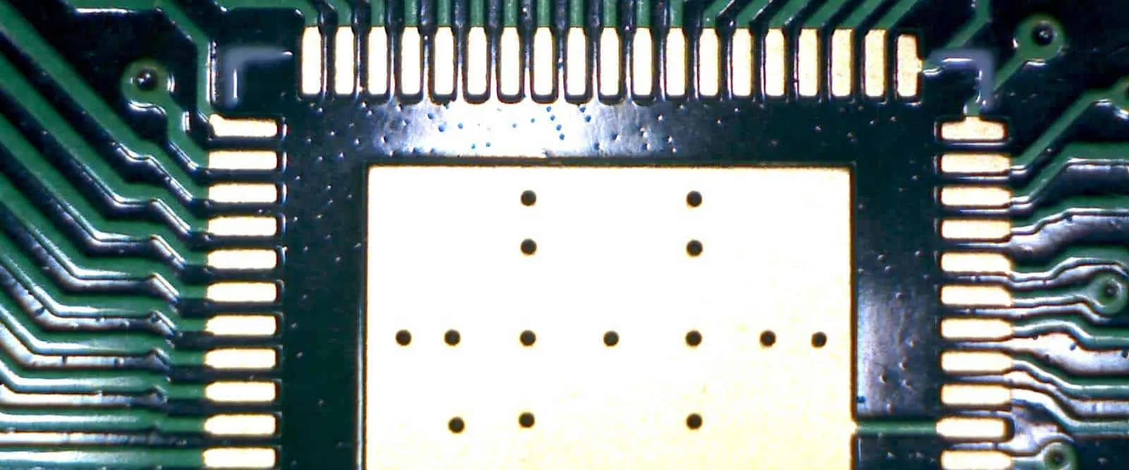
Copper pour fills unused blank areas of a PCB with copper. It is also sometimes called copper flooding. The step is more important than it first appears. It can reduce ground impedance and improve the board's immunity to interference. It can also reduce voltage drop and improve power delivery efficiency. When the pour is tied to ground, it can reduce loop area. PCB fabricators also have a requirement here: pouring copper in open areas helps keep the board from warping during soldering. The practice is therefore a need of both design and manufacturing.
Unbalanced copper is one reason boards bow in the press and again in soldering. A side or a region with little copper shrinks differently from a side covered by planes. Filling open areas evens that copper distribution and reduces the warp that later shows up as poor solder joints. That manufacturing reason exists even on boards that do not need the pour for current or shielding.
There is an important condition: a poorly implemented pour is worse than no pour at all. In high-frequency circuits in particular, if the poured copper is not grounded properly, copper that should act as a shield can become a path that helps noise propagate. A floating or weakly tied region couples to the nets it surrounds, then re-radiates or carries that energy to another part of the board. Leaving the area empty avoids that extra conductor.
One related point is worth noting. When a trace length is greater than 1/20 of the wavelength corresponding to the noise frequency, an antenna effect can occur and noise can be radiated. After copper is poured on a high-frequency board, stitching vias must therefore be placed at a spacing smaller than λ/20 so the pour is well connected to the ground plane. This step should not be skipped.
The λ/20 spacing is a connection rule, not a decoration. A via stitch ties the pour to the reference plane often enough that no segment of the pour is long enough to act as an antenna at the noise frequency of concern. Wider spacing leaves copper islands that are electrically long. Those islands are the path that turns a shield into a radiator. The same limit explains why a long trace on a high-frequency board can radiate once its length exceeds 1/20 of the noise wavelength: the conductor is no longer a lumped connection.
Solid Copper Pour
Solid copper pour, also called large-area copper fill, is often the first choice in low-frequency designs. Its advantages are clear: it can increase current-carrying capacity and provide strong electromagnetic shielding. For circuits that must handle high current, it is highly practical.
Continuous copper has more cross-section than a grid of the same outline. Voltage drop along a power or ground pour falls as that cross-section rises, which is why a solid fill supports power delivery better than a hatch of the same outer shape. The continuous sheet is also the stronger shield. There are no openings for field leakage at the scale of the grid, and return current has a broad path instead of a set of narrow traces.
It also has a drawback. During wave soldering, a large copper area expands as it heats, which can warp the board or even cause the copper foil to blister. The issue is straightforward to address: add slots in the large poured area during design to relieve thermal deformation and avoid this problem.
The slots break the continuous sheet into regions that can expand without buckling the foil or bowing the laminate. They are thermal-relief features in the pour, not signal slots. Placing them without cutting the current path into a narrow neck preserves the capacity that made the solid pour attractive. A solid fill with no relief is the pattern most likely to blister or warp in wave soldering. A solid fill with relief slots keeps the current and shield benefits while giving the copper room to move.
Hatched Copper Pour
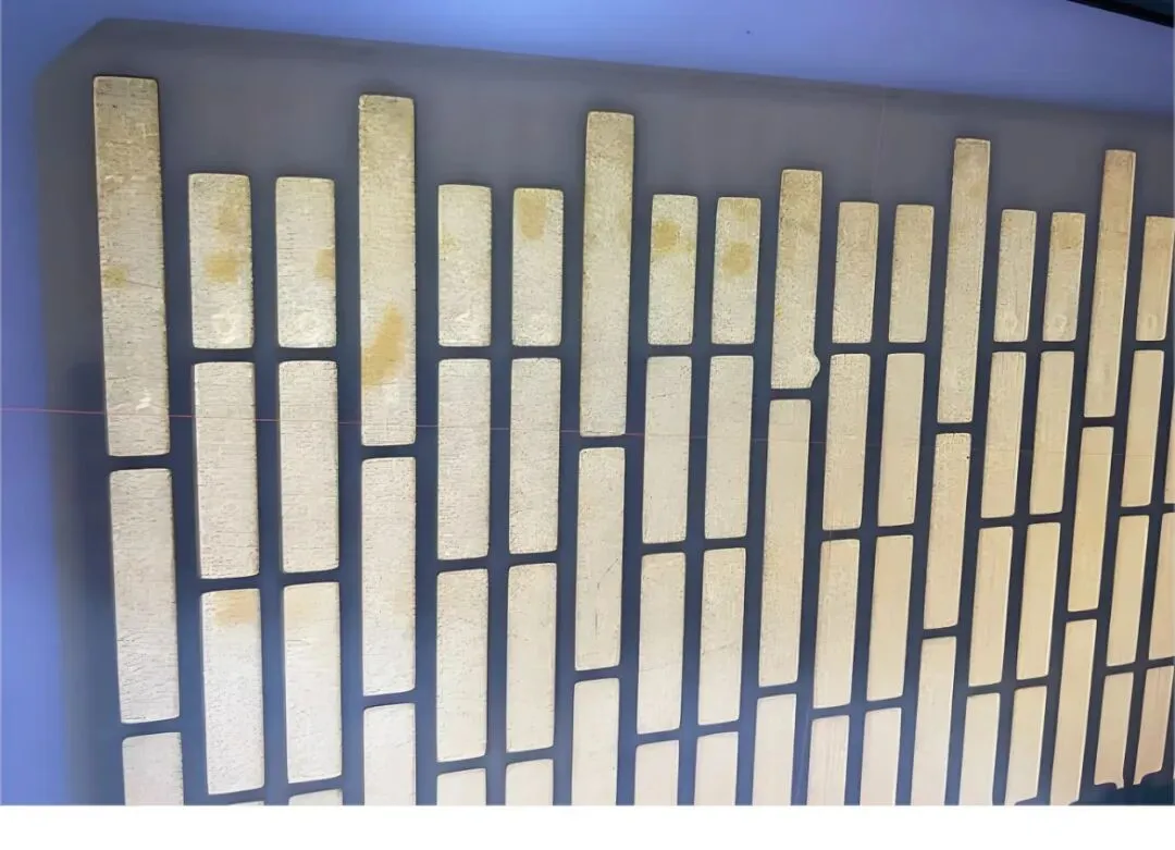
The primary role of hatched copper pour is shielding. Compared with solid pour, its ability to carry higher current is much weaker, so it should not be the first choice for high-current circuits. The grid replaces a sheet with a set of traces. Current crowds into those traces, voltage drop rises, and the pour stops being a power-distribution feature.
Its advantages are still significant. Heat dissipation is much better than with solid pour because the grid reduces the heated copper area, so heating during soldering is more uniform and soldering problems are less likely. Less copper mass reaches reflow or wave temperature, and the openings give the board a more even thermal load than a broad sheet that sinks heat at the edges and blisters in the center.
Hatched pour is also commonly used in touch circuits, where the shielding performance is sufficient for that class of design. Touch electrodes and nearby sense nets need a shield that does not present the full capacitive load of a solid sheet. A hatch can provide that lighter shield when the grid is fine enough for the interference being blocked and coarse enough not to recreate a solid plane.
One important caution applies. A hatch is made of crossing traces, and those traces have an electrical length related to the board's operating frequency. At low operating frequencies this is usually not obvious. If the electrical length matches the operating frequency, the circuit can radiate interference widely and may no longer operate correctly. This must be considered during design.
Each leg of the grid is a conductor. If that leg, or a loop formed by crossing legs, is an appreciable fraction of a wavelength at the operating frequency, the hatch behaves as a set of antennas rather than as a shield. The same λ/20 concern that drives stitching vias on a solid high-frequency pour applies to the hatch geometry itself. A hatch copied from a low-frequency board onto a faster design can be the source of the interference the pour was added to stop.
Selection Guideline
The core selection rule can be applied directly:
- Low-frequency, high-current circuits: use solid copper pour, and add thermal relief slots to avoid blistering.
- High-frequency circuits with high immunity requirements, touch circuits, or designs with thermal constraints: use hatched copper pour, and match the hatch to the operating frequency so electrical length does not create interference.
Low frequency plus high current favors the solid sheet because capacity and shielding both improve, and the wavelength is long enough that a slotted plane is not an antenna. High frequency, touch sensing, and boards that cannot tolerate the thermal mass of a solid fill favor the hatch, provided the grid is checked against the operating frequency and the pour is stitched.
Grounding is not optional in either case. Stitching vias at a spacing smaller than λ/20 keep a high-frequency pour from becoming a noise path. A hatch whose traces are electrically long at the operating frequency fails the same way, even if every end of the grid is tied down.
PCB copper pour is never a one-size-fits-all choice. There is no need to lock onto a single style. Choose according to how the board actually operates, and ground the pour correctly. Only then can copper pour increase current-carrying capability and shield interference at the same time, and help keep board performance more stable.