 00:47
00:47
PCB Stackup Design
PCB stackup design is a fundamental aspect of printed circuit board engineering that determines the arrangement of conductive and insulating layers within a PCB. This configuration plays a critical role in ensuring signal integrity, managing electromagnetic interference, and optimizing thermal performance in electronic devices. For engineers and designers searching for insights on PCB stackup design, this tag aggregates resources that delve into the principles and methodologies for creating effective multilayer boards, from simple two-layer setups to complex high-speed applications. Understanding PCB stackup design begins with selecting appropriate layer counts, materials, and via structures to meet specific project requirements. Key considerations include controlled impedance for high-frequency signals, power distribution planes to minimize noise, and ground layers for shielding. Practical applications span industries such as telecommunications, automotive electronics, and consumer gadgets, where poor stackup can lead to issues like crosstalk or signal degradation. Best practices emphasize simulation tools for pre-layout analysis, adherence to manufacturing constraints, and iterative testing to refine designs, ultimately reducing prototyping costs and time to market. Articles under this tag offer detailed guides on topics like symmetric versus asymmetric stackups, the impact of dielectric constants on performance, and strategies for high-density interconnects. Whether you are troubleshooting a current project or planning a new one, these resources provide actionable steps to enhance your PCB designs. Dive into the collection to find case studies, tutorials, and expert tips that align with real-world challenges in electronics development.
Video Guide

Technical Articles
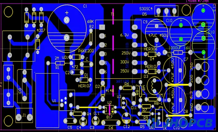
Cost Effective PCB Trace Routing: Strategies for Reducing Manufacturing Costs
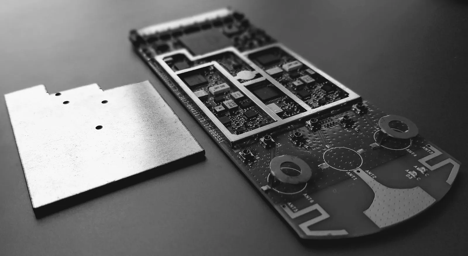
The Case For Using Copper Pour On Routing Layers

6G Massive MIMO: Key Technical Trends
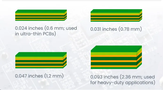
Thick vs. Thin: Decoding PCB Thickness for Your Next Electronic Project

Signal Integrity Secrets: How Thick PCBs Minimize EMI and Crosstalk in High-Speed Circuits
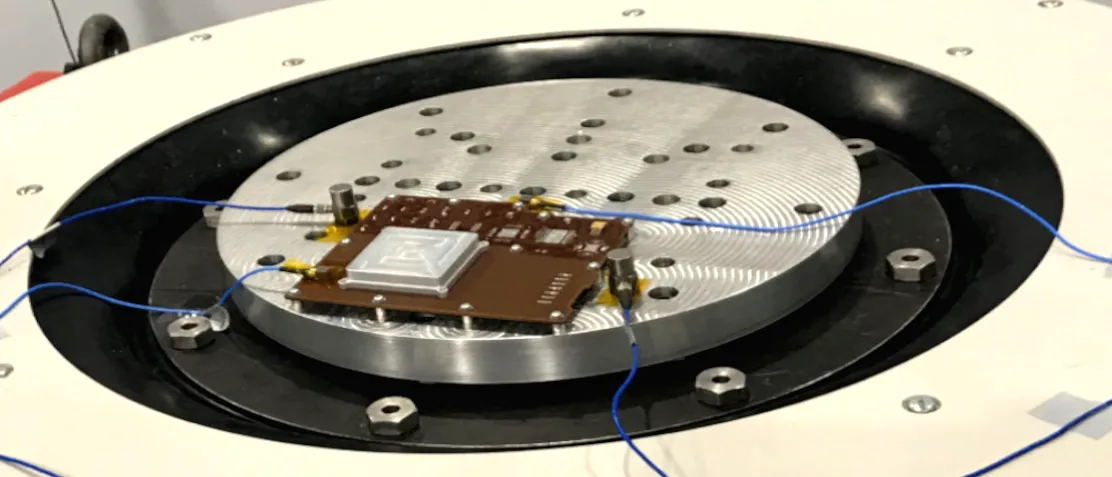
The Impact of Layer Thickness on PCB Mechanical Stability and Reliability
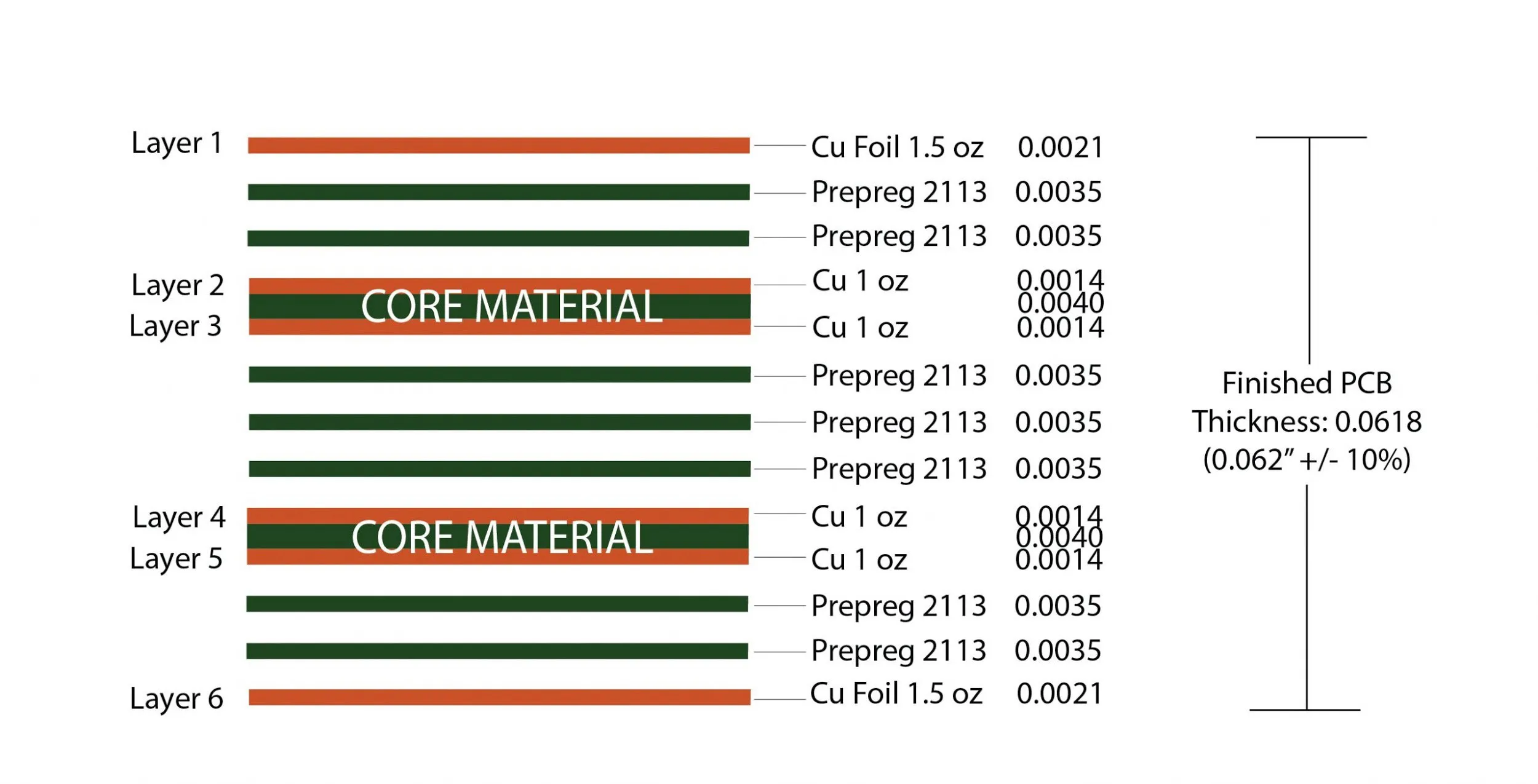
Achieving Controlled Impedance: The Role of Layer Thickness in PCB Design
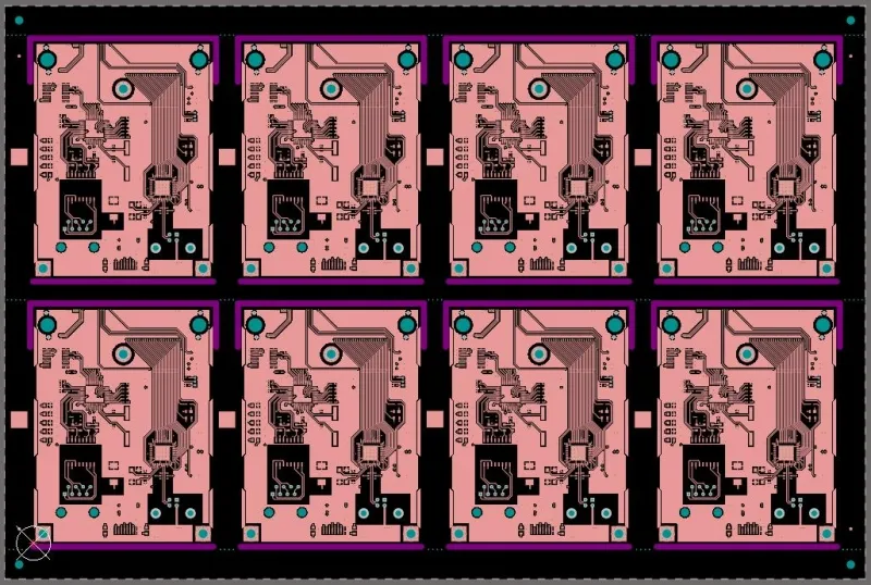
PCB Panel Size and Impedance Control: Design Considerations
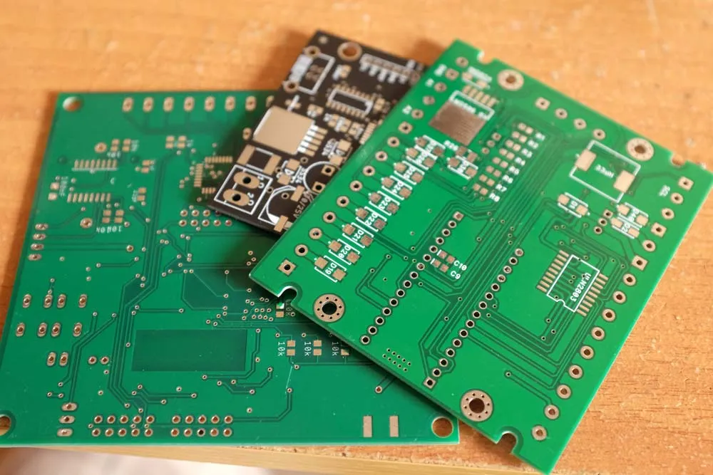
Unlocking Miniaturization: A Comprehensive Guide to Thin PCB Technology
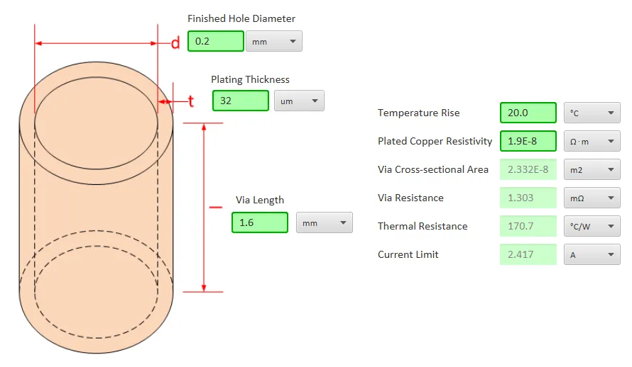
The Impact of PCB Aspect Ratio on Signal Integrity: A Deep Dive for High-Speed Designs
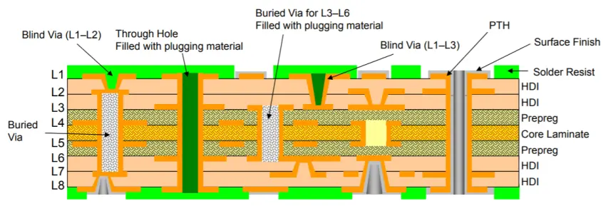
PCB Aspect Ratio and Thermal Management: Keeping Your Boards Cool and Reliable
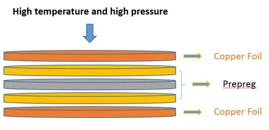
Choosing the Right Copper Clad Laminate (CCL): A Comprehensive Guide
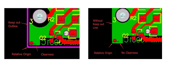
Mastering PCB Outlines: A Comprehensive Guide for Electrical Engineers
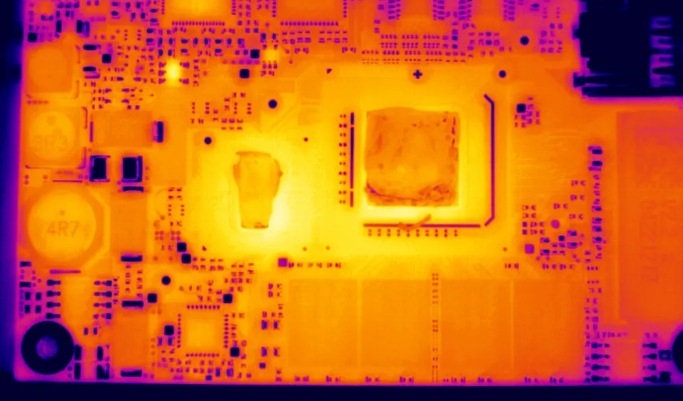
Thermal Runaway: Managing Heat Dissipation in Maximum Sized PCBs
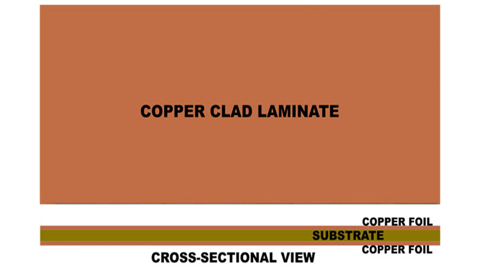
Maximizing Signal Integrity: The Role of Copper Cladding in High-Frequency PCBs
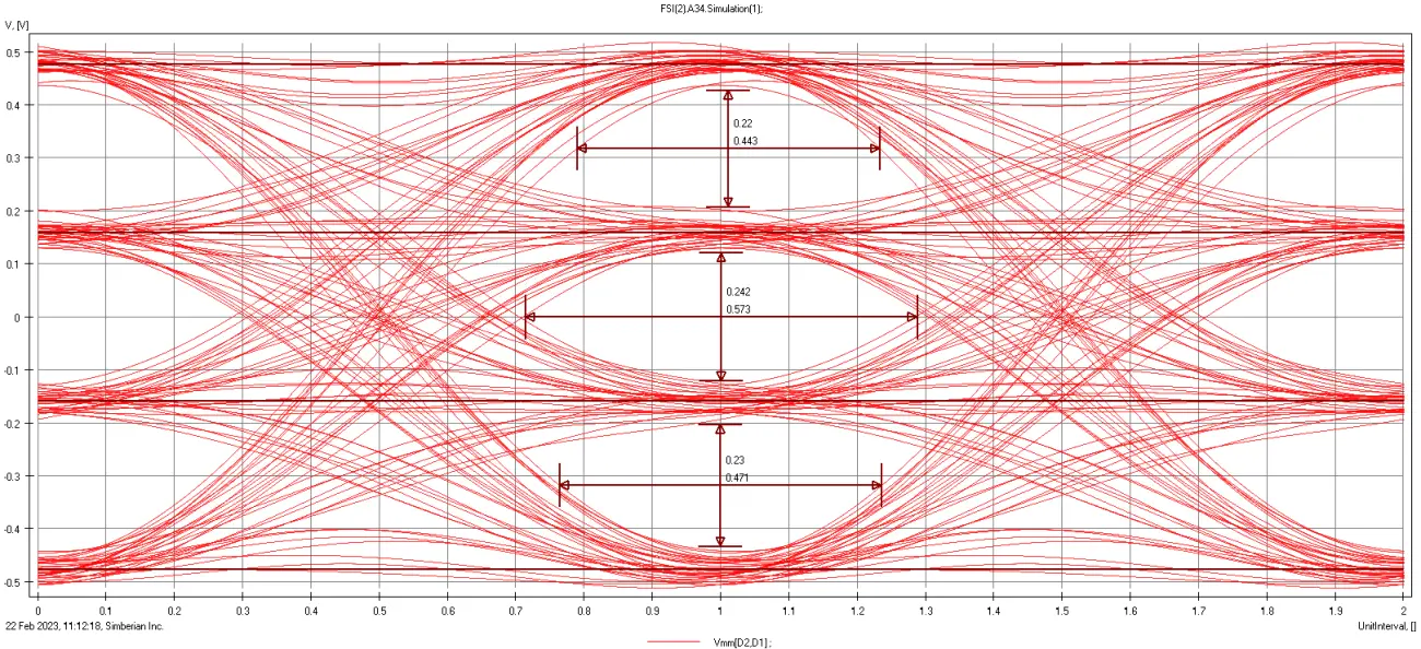
The Signal Integrity Gamble: How PCB Size Affects High-Speed Performance
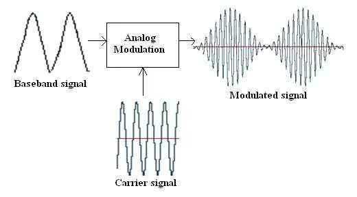
RF Modulation Techniques: PCB Design and Manufacturing Considerations for Wireless Communication Systems
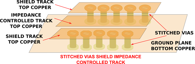
Via Stitching and Copper Balancing: A Symbiotic Relationship for Superior PCB Performance
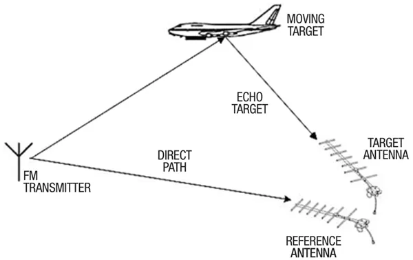
Types of Passive Radar Receivers