Introduction
In high-speed PCB design, maintaining signal quality is paramount as data rates climb into gigabits per second. The PCB aspect ratio, defined as the ratio of board thickness to the smallest via drill diameter, plays a subtle yet critical role in this process. High aspect ratios can introduce manufacturing challenges that degrade signal integrity through increased attenuation and impedance mismatches. Engineers must understand these effects to optimize designs for reliable performance. This article explores the mechanisms linking PCB aspect ratio to signal integrity issues and offers practical strategies for mitigation. By adhering to established guidelines, designers can enhance high-speed PCB design outcomes.
What Is PCB Aspect Ratio and Why Does It Matter for Signal Integrity?
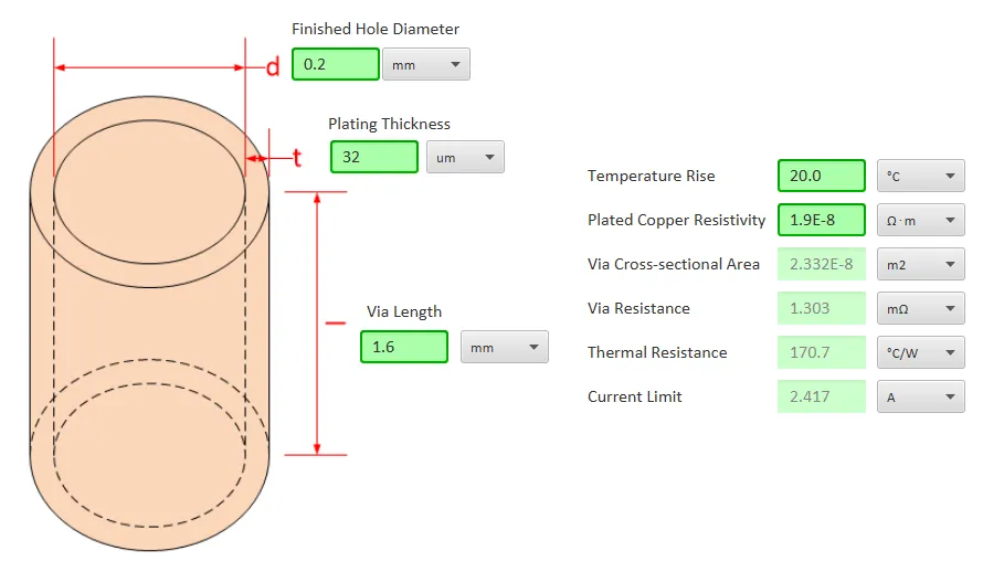
PCB aspect ratio refers to the proportion between the total board thickness and the diameter of the smallest drilled via hole. This metric directly influences the feasibility of uniform plating during fabrication. Industry standards, such as IPC-2221, emphasize keeping aspect ratios within manageable limits to ensure plating quality. In high-speed designs, where signals traverse multiple layers via these structures, any deviation in via integrity can propagate errors.
Excessive aspect ratios complicate electroplating, leading to thinner copper deposits at the via bottom. This results in higher electrical resistance, which manifests as signal attenuation over long paths. Moreover, uneven plating creates local impedance variations, fostering reflections that distort waveforms. For electric engineers tackling PCB aspect ratio signal integrity, recognizing these risks early prevents costly respins. Ultimately, a balanced aspect ratio supports consistent signal quality across the board.
The Technical Mechanisms: How Aspect Ratio Affects Signal Integrity
High PCB aspect ratios challenge the plating process because electrolytic copper deposition struggles to penetrate deeply into narrow, elongated holes. As the ratio exceeds recommended thresholds, copper thickness tapers toward the via center, increasing DC and AC resistance. In high-speed PCB design, this resistance contributes to signal attenuation, where high-frequency components lose amplitude progressively. Skin effect exacerbates the issue, confining current to the via walls and amplifying losses from thin plating.
Impedance mismatch arises when plating nonuniformity alters the via's effective diameter along its length. Such discontinuities cause signal reflections, ringing, and eye diagram closure at receiver ends. Thicker boards with high aspect ratios also promote warpage during lamination and cooling, mechanically stressing traces and vias. This stress induces microcracks or delamination, further disrupting controlled impedance profiles essential for signal quality.
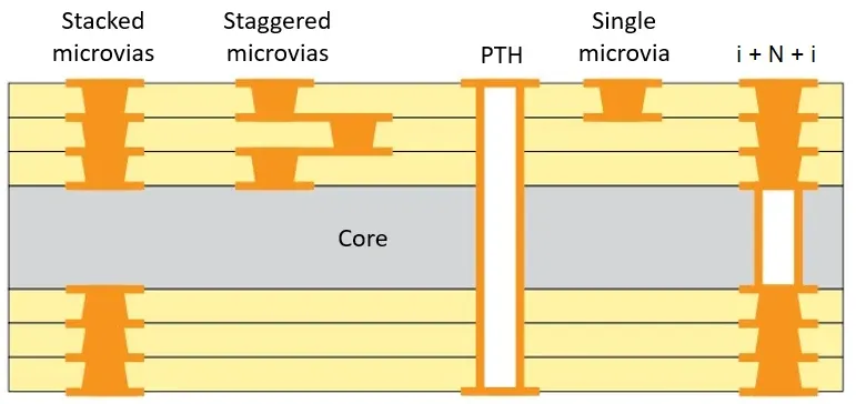
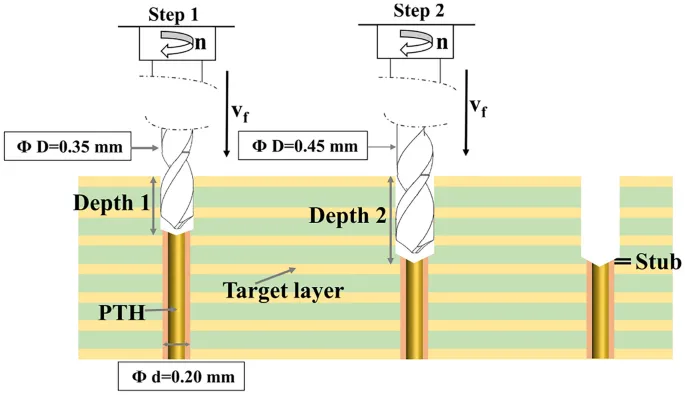
Via stubs in multilayer boards represent another concern tied to board thickness. Longer stubs from thicker constructions resonate at frequencies relevant to high-speed signals, injecting noise and attenuation. Fabricators must backdrill or use blind vias to shorten stubs, but high aspect ratios limit viable drill sizes. Collectively, these mechanisms underscore why PCB aspect ratio signal integrity demands careful stackup planning.
Key Effects on High-Speed Signals: Attenuation and Mismatch in Detail
Signal attenuation in high aspect ratio vias stems primarily from elevated series resistance. At multi-GHz frequencies, dielectric losses compound with conductor losses, narrowing the signal bandwidth. Engineers observe this as intersymbol interference in serial links, where attenuated edges fail to resolve properly. Maintaining low aspect ratios ensures robust plating, minimizing these losses and preserving signal quality.
Impedance mismatch, a frequent byproduct, occurs at via transitions where plating voids create capacitive or inductive lumps. Reflections from these mismatches degrade return loss, pushing it beyond acceptable -10 dB thresholds. In differential pairs, asymmetric via plating worsens common-mode conversion, amplifying crosstalk. High-speed PCB design simulations must model these effects accurately to predict real-world performance.
Warpage from thick, high-ratio boards alters trace-to-plane spacing, varying characteristic impedance across the panel. This spatial nonuniformity leads to deterministic jitter in clock signals. Standards like IPC-6012 address board quality to mitigate such variations, but design choices set the foundation. Addressing PCB aspect ratio signal integrity holistically integrates fabrication feedback loops.
Practical Solutions and Best Practices for High-Speed PCB Design
To counter high aspect ratio pitfalls, prioritize thinner stackups where possible, targeting aspect ratios below 8:1. Select larger via drill diameters for through-holes, balancing density with manufacturability. For dense high-speed nets, employ blind or buried vias, which inherently feature lower aspect ratios due to shorter depths. Backdrilling extends this benefit by removing stubs, though it requires precise depth control.
Layer count optimization reduces overall thickness without sacrificing routing channels. Use via-in-pad or filled vias for transitions, minimizing stub lengths and inductance. Simulate via models incorporating realistic plating profiles to forecast impedance mismatch and signal attenuation. Collaborate with fabricators early to validate aspect ratio feasibility against their capabilities.
Incorporate ground stitching vias densely around high-speed signals to stabilize return paths and reduce crosstalk. Maintain symmetric stackups to curb warpage, ensuring uniform dielectric spacing for consistent impedance. These practices elevate signal quality in high-speed PCB design, aligning with IPC guidelines for reliable performance.
Troubleshooting Common Issues in High Aspect Ratio Designs
Engineers often encounter signal degradation post-fabrication when aspect ratios push limits. Eye diagram analysis reveals attenuation through reduced height and width; TDR traces pinpoint impedance mismatches at vias. Warpage inspections using shadow moire confirm mechanical contributors. Mitigate by redesigning with microvias or laser-drilled structures for finer features.
Fabrication reviews should scrutinize plating coupons for uniformity. If attenuation persists, section vias for SEM analysis of copper thickness. Adjust designs iteratively, favoring lower ratios. This structured troubleshooting preserves PCB aspect ratio signal integrity.
Conclusion
PCB aspect ratio profoundly influences signal integrity in high-speed designs through plating quality, resistance, and mechanical stability. High ratios amplify signal attenuation and impedance mismatch, compromising performance. By selecting appropriate drill sizes, via types, and stackups, engineers can uphold signal quality. Adhering to standards ensures manufacturability and reliability. Prioritizing these factors yields robust high-speed PCB designs ready for demanding applications.
FAQs
Q1: What is the ideal PCB aspect ratio for high-speed signal integrity?
A1: In high-speed PCB design, aim for aspect ratios under 8:1 to ensure uniform via plating and minimize signal attenuation. Thicker boards necessitate larger drills to maintain this, preventing impedance mismatch. IPC-2221 provides guidelines for balancing density and reliability. This approach sustains signal quality across frequencies.
Q2: How does high PCB aspect ratio cause impedance mismatch?
A2: High ratios lead to thinner plating at via bottoms, creating diameter variations that disrupt characteristic impedance. Reflections from these discontinuities degrade signal quality in high-speed nets. Simulations and TDR verify issues early. Optimizing via design counters this effect effectively.
Q3: Can signal attenuation be reduced in thick PCBs with high aspect ratios?
A3: Yes, by using backdrilling, blind vias, or filled structures to shorten paths and improve plating. These reduce resistance losses critical for high-speed PCB design. Thinner dielectrics also help maintain low aspect ratios. Consistent signal quality follows from such strategies.
Q4: Why is PCB aspect ratio signal integrity crucial for electric engineers?
A4: It directly impacts via reliability, affecting attenuation and reflections in multi-GHz signals. Poor control leads to eye closure and jitter. Best practices like symmetric stackups mitigate risks. Engineers achieve superior signal quality through proactive design.
References
IPC-2221B — Generic Standard on Printed Board Design. IPC, 2012
IPC-6012E — Qualification and Performance Specification for Rigid Printed Boards. IPC, 2017
IPC-A-600K — Acceptability of Printed Boards. IPC, 2020
J-STD-001H — Requirements for Soldered Electrical and Electronic Assemblies. IPC, 2018


