Introduction
In modern electronics, printed circuit boards face increasing thermal challenges from higher power densities and compact designs. PCB aspect ratio, defined as the ratio of board thickness to the smallest drilled hole diameter, plays a pivotal role in thermal management. A well-optimized aspect ratio ensures effective heat dissipation paths through vias and the board itself, preventing hot spots that compromise component reliability. Poorly managed aspect ratios can lead to plating defects in vias, exacerbating thermal resistance and CTE mismatch issues during operation. This article explores how PCB aspect ratio thermal management influences overall board performance, offering engineers structured insights for reliable designs. By balancing manufacturability with thermal needs, designers can enhance longevity and efficiency.
Understanding PCB Aspect Ratio and Its Thermal Implications
PCB aspect ratio directly affects the quality of via plating and the board's inherent thermal properties. Typically calculated as board thickness divided by via or through-hole diameter, standard ratios range from 5:1 to 10:1 depending on fabrication capabilities. Higher ratios challenge electroplating processes, resulting in thinner copper walls that increase thermal resistance in heat transfer paths. Thicker boards, which elevate the aspect ratio for fixed hole sizes, provide greater thermal mass for spreading heat laterally across the plane. This interplay is critical in PCB aspect ratio thermal management, as it determines how efficiently heat moves from components to sinks or ambient air. Engineers must consider these factors early to avoid reliability failures in high-power applications.
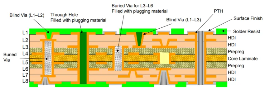
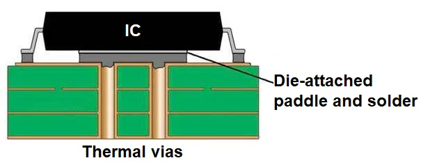
Thermal vias, essential for channeling heat from surface components to inner layers or the opposite side, are particularly sensitive to aspect ratio. A high aspect ratio via may suffer from incomplete filling or voiding, reducing its conductance and creating localized hot spots. Conversely, optimal ratios ensure robust plating, maintaining low thermal impedance. Board thickness also influences convection and radiation cooling surfaces. In multilayer stacks, cumulative effects amplify these concerns, demanding precise control.
Technical Mechanisms Linking Aspect Ratio to Heat Dissipation
Heat dissipation in PCBs relies on conduction through copper features, vias, and the substrate, all modulated by aspect ratio. Vias act as thermal bridges, but their effectiveness diminishes with higher aspect ratios due to longer conduction paths and potential plating nonuniformity. The thermal resistance of a via barrel increases proportionally with length-to-diameter ratio, as per basic heat transfer principles. This can elevate junction temperatures in power components, accelerating degradation mechanisms like electromigration. Hot spots emerge when heat concentrates around inadequately cooled areas, further stressing nearby elements.
CTE mismatch compounds these issues, especially in thermal cycling environments. Copper plating expands differently from the dielectric core, generating shear stresses at interfaces. High aspect ratio vias experience amplified stress concentrations along elongated barrels, risking cracks or delamination over cycles. IPC-2221 guidelines emphasize aspect ratio limits to mitigate such risks, recommending ratios below 10:1 for reliable plating and thermal performance. Component reliability suffers as elevated temperatures reduce mean time between failures, following Arrhenius models where every 10-degree rise halves lifespan. Understanding these mechanisms allows engineers to predict and prevent failures systematically.
Board-level heat spreading benefits from thicker substrates, which offer larger cross-sections for lateral conduction. However, excessive thickness raises aspect ratios, trading one advantage for manufacturing hurdles. In dense designs, this balance dictates plane usage for isothermal spreading. Radiation and convection scale with exposed surface area, indirectly tying back to thickness choices.
Best Practices for Optimizing PCB Aspect Ratio Thermal Management
Start with design rules that cap aspect ratios at manufacturable levels, typically 8:1 to 12:1 for advanced processes. Select via diameters to match board thickness, prioritizing larger drills for thermal vias under power devices. Array thermal vias in 3x3 or larger patterns around heat sources, tenting unused ones to prevent solder wicking while preserving paths. Filled or plugged vias further enhance conductance by eliminating air gaps, ideal for high-reliability applications.
Material selection addresses CTE mismatch proactively. Low-CTE laminates minimize differential expansion with copper, reducing stress in high aspect ratio features. Increase copper weights in planes and pours to boost spreading capacity, calculating thermal conductivity via k = thickness * copper fraction. IPC-6012 specifications guide qualification for thermal performance, ensuring boards withstand operational stresses. Simulate early using finite element analysis to visualize gradients and iterate layouts.
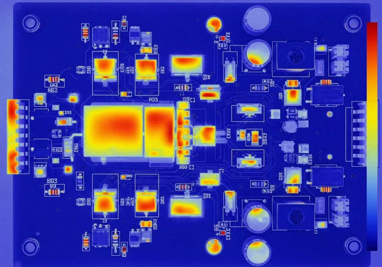
Layer stacking influences vertical heat flow, positioning ground planes near hot components for sinking. Edge connectors or heatsinks benefit from beveled profiles to maximize contact. During layout, space high-power parts to leverage natural airflow, avoiding clusters that amplify hot spots. Post-design verification through infrared imaging confirms dissipation efficacy before production.
Troubleshooting Common Thermal Issues Tied to Aspect Ratio
Engineers often encounter elevated temperatures traceable to suboptimal aspect ratios. Symptoms include via barrel cracking post-reflow or inconsistent power delivery from thermal throttling. Inspect cross-sections for plating thickness uniformity; thin walls signal high-ratio problems. Warpage from CTE mismatch manifests as bow exceeding 0.75% of panel dimension, per industry norms.
Mitigate by redesigning with staggered via sizes or blind/buried alternatives to shorten paths. Reflow profiling per JEDEC J-STD-020 minimizes peak exposures that exacerbate stresses. Prototype testing under load reveals hot spots via thermocouples, guiding refinements. Document lessons to refine design rules for future iterations.
Conclusion
Mastering PCB aspect ratio thermal management ensures boards remain cool and reliable under demanding conditions. By optimizing ratios for via integrity, leveraging thermal vias, and addressing CTE mismatch, engineers enhance heat dissipation and component reliability. Practical strategies like simulation, material choices, and standard adherence yield robust designs. Prioritizing these elements minimizes hot spots and extends service life. Future trends in high-density interconnects will amplify the need for such precision, rewarding proactive thermal planning.
FAQs
Q1: What role do thermal vias play in PCB aspect ratio thermal management?
A1: Thermal vias transfer heat vertically through the board, but their performance hinges on aspect ratio. Lower ratios ensure thicker plating for better conductance, reducing resistance. Arrays around components prevent hot spots, with patterns optimized via simulation. This approach boosts overall heat dissipation while maintaining manufacturability.
Q2: How does CTE mismatch affect high aspect ratio PCBs?
A2: CTE mismatch induces stresses during thermal cycling, cracking high aspect ratio via barrels due to expansion differences. Thinner plating amplifies vulnerabilities, leading to reliability failures. Select matched materials and limit ratios per IPC guidelines to distribute stresses evenly. This preserves component reliability in varying environments. (58 words)
Q3: Why are hot spots a concern in PCB thermal management?
A3: Hot spots arise from poor heat dissipation, concentrating temperatures that degrade components nearby. High aspect ratios worsen this by impeding via paths. Mitigate with copper planes, thermal vias, and airflow optimization to uniformize profiles. Consistent temperatures enhance longevity and performance. (48 words)
Q4: How can engineers improve heat dissipation on thick PCBs?
A4: Thick boards offer thermal mass but raise aspect ratios, challenging vias. Use larger diameters, filled vias, and inner planes for spreading. Simulate to balance thickness with cooling needs. Adhering to standards ensures reliable outcomes without excessive costs. (46 words)
References
- IPC-2221B — Generic Standard on Printed Board Design. IPC, 2012
- IPC-6012E — Qualification and Performance Specification for Rigid Printed Boards. IPC, 2015
- JEDEC J-STD-020E — Moisture/Reflow Sensitivity Classification of Nonhermetic Surface Mount Devices. JEDEC, 2014


